Variable-size solder bump structures for integrated circuit packaging

a technology of integrated circuit packaging and solder bumps, which is applied in the direction of printed circuit manufacturing, printed circuit aspects, and testing/measurement of semiconductor/solid-state devices, etc., can solve the problems of reducing the planarity warping and affecting the electrical connection provided, so as to improve the yield of the ic package

Active Publication Date: 2014-05-22
NVIDIA CORP
View PDF46 Cites 14 Cited by
  • Summary
  • Abstract
  • Description
  • Claims
  • Application Information

AI Technical Summary

Benefits of technology

[0011]One advantage of the disclosed technique is that variable-size solder bump structures and variable solder paste volumes may be utilized to salvage IC packages which would otherwise be discarded as being outside of a coplanarity specification. The coplanarity of these IC packages may be corrected, and the resulting IC package may be successfully surface mounted to a circuit board or other type of substrate, improving IC package yields.

Problems solved by technology

Consequently, IC packaging techniques have encountered challenges for providing packaging which supports the requisite number of electrical connections.
Upon cooling, a mismatch between the CTE of the die and the CTE of the substrate may cause the substrate to warp, reducing the planarity of the IC package and preventing electrical connections from being formed with the IC package.
Additionally, warping of the IC package may affect the electrical connections provided between the die and the substrate.

Method used


Image

  • Variable-size solder bump structures for integrated circuit packaging
  • Variable-size solder bump structures for integrated circuit packaging
  • Variable-size solder bump structures for integrated circuit packaging

Examples


Embodiment Construction

[0018]In the following description, numerous specific details are set forth to provide a more thorough understanding of embodiments of the present invention. However, it will be apparent to one of skill in the art that embodiments of the present invention may be practiced without one or more of these specific details.

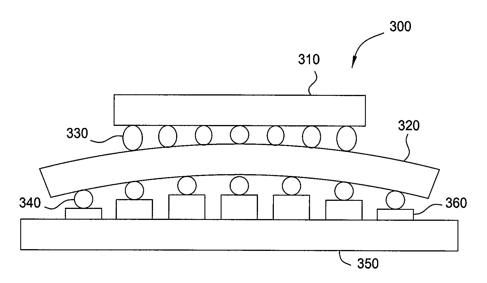
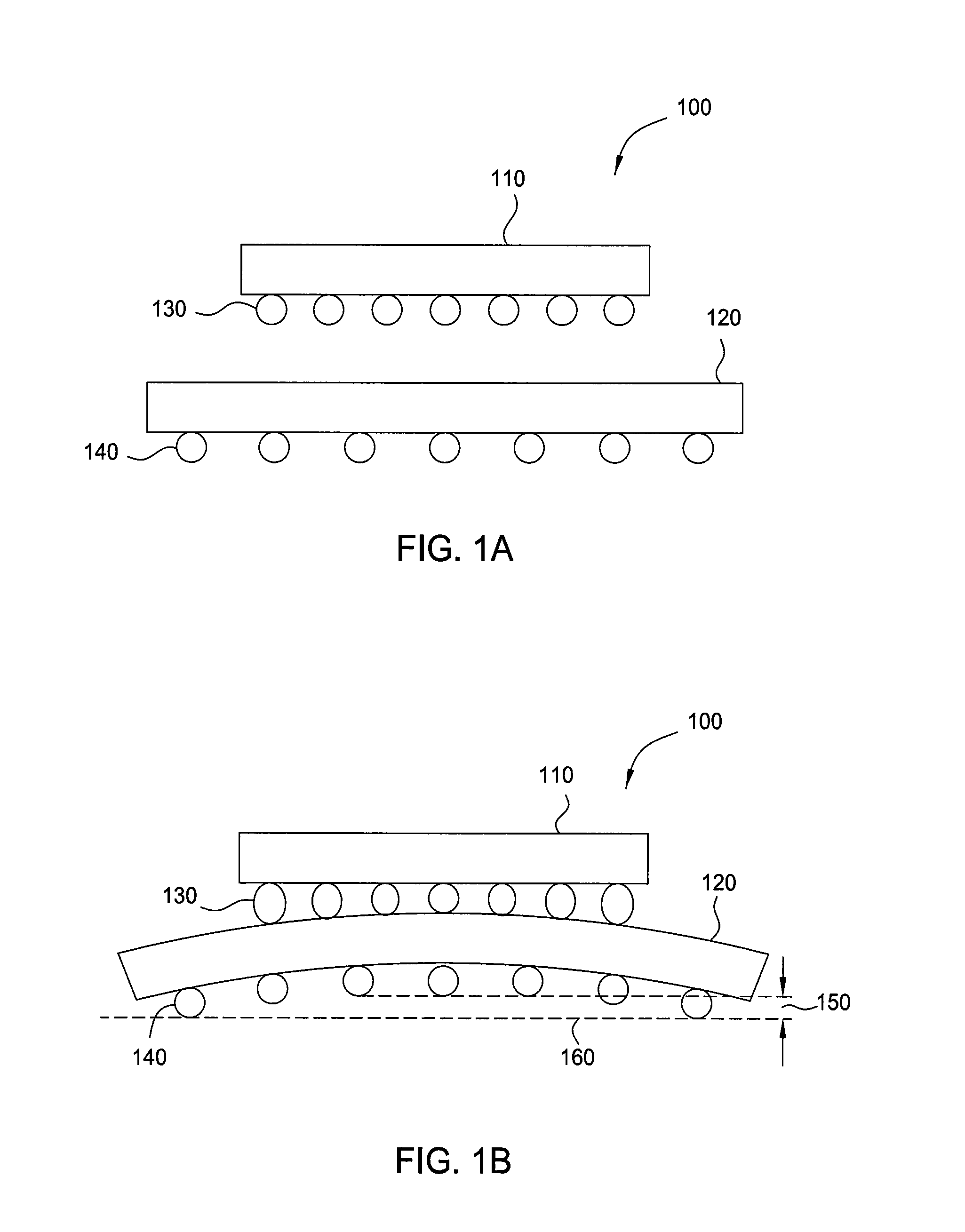
[0019]FIGS. 1A and 1B illustrate schematic views of an integrated circuit (IC) package 100 having a conventional configuration. The conventional IC package 100 includes a die 110, a substrate 120, a first plurality of solder balls 130, and a second plurality of solder balls 140. The first plurality of solder balls 130 mechanically and electrically couple the die 110 to the substrate 120 and provide electrical connections between the die 110 and the substrate 120. The second plurality of solder balls 140 mechanically and electrically couple the conventional IC package 100 to a circuit board (not shown) and provide electrical connections between the conventional IC packag...


PUM


Abstract

One embodiment of the present invention sets forth an integrated circuit package including a substrate, an integrated circuit die, a first plurality of solder bump structures, and a first plurality of variable-size solder bump structures. The first plurality of solder bump structures electrically couple the integrated circuit die to the substrate. The first plurality of variable-size solder bump structures are disposed on a bottom surface of the substrate. The first plurality of variable-size solder bump structures are sized to be substantially coplanar with a seating plane of the integrated circuit package.

Description

BACKGROUND OF THE INVENTION[0001]1. Field of the Invention[0002]Embodiments of the present invention generally relate to fabricating and surface mounting integrated circuit packages.[0003]2. Description of the Related Art[0004]Integrated circuit (IC) fabrication is a multi-step sequence which includes processes such as patterning, deposition, etching, and metallization. Typically, in the final processing steps, the resulting IC die are separated and packaged. IC packaging serves several purposes, including providing an electrical interface with the die, providing a thermal medium through which heat may be removed from the die, and / or providing mechanical protection for the die during subsequent usage and handling.[0005]One type of IC packaging technique is referred to as “flip chip” packaging. In flip chip packaging, after the metallization process is complete, solder bump structures (e.g., solder balls, pads, etc.) are deposited on the die, and the die is separated from the wafer (...

Claims


Application Information

Patent Timeline
Patent Type & Authority Applications(United States)
IPC IPC(8): H01L23/00
CPCH01L24/17H01L24/81H01L22/12H01L22/20H01L2224/831H01L23/49816H01L24/13H01L24/14H01L24/16H01L2224/131H01L2224/1403H01L2224/16225H01L2224/73204H01L2224/81815H01L2924/15311H01L2224/81048H05K3/3436H05K2201/10674H01L23/49811H01L2924/07802H01L21/563H01L2924/3511H01L2224/1703H01L2924/00014H01L2924/014H01L2924/00
Inventor ZHANG, LEILEIBOKHAREY, ZUHAIR
Owner NVIDIA CORP
Why Eureka
Try Eureka