Organic Light Emitting Display Device
a light-emitting display and organic technology, applied in the field of organic light-emitting display devices, can solve the problems of devices that cannot realize uniform image quality, and achieve the effect of increasing current efficiency
- Summary
- Abstract
- Description
- Claims
- Application Information
AI Technical Summary
Benefits of technology
Problems solved by technology
Method used
Image
Examples
first embodiment
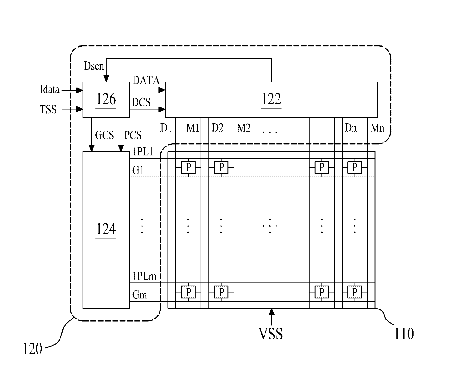
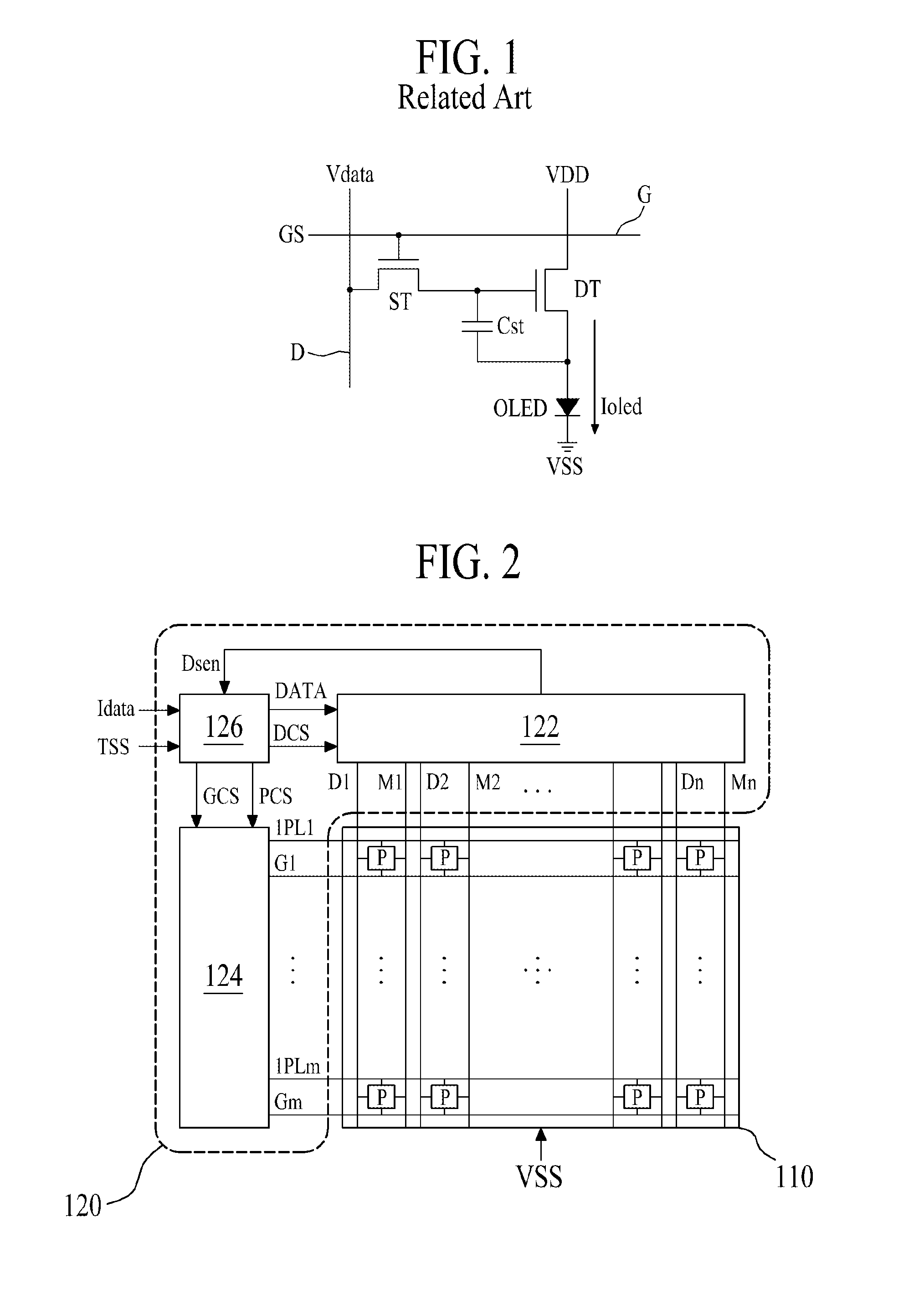
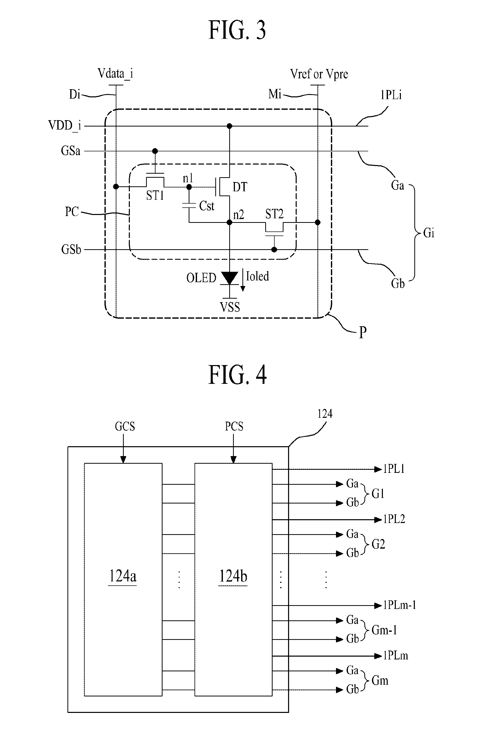
[0048]FIG. 2 is a diagram for describing an organic light emitting display device and FIG. 3 is a circuit diagram for describing a pixel structure of FIG. 2.
[0049]With reference to FIGS. 2 and 3, the organic light emitting display device according to the first embodiment may include a display panel 110 and a panel driver 120.
[0050]The display panel 110 may include a plurality of pixels P that are selectively driven in a data charging period, in which a difference voltage “Vdata−Vref” between a data voltage Vdata (shown in FIG. 3 as Vdata_i, which is the data voltage Vdata supplied to an ith data line Di) and a reference voltage Vref is charged into a capacitor Cst connected between a gate and source of a driving transistor DT receiving a first driving voltage VDD_i, and a light emitting period in which an light emitting element OLED emits light with a data current Ioled that flows from a first driving voltage VDD_i terminal to a second driving voltage VSS terminal through a driving...
second embodiment
[0147]FIG. 16 is a diagram for describing an organic light emitting display device and FIG. 17 is a circuit diagram for describing a pixel structure of FIG. 16.
[0148]With reference to FIGS. 16 and 17, the organic light emitting display device according to the second embodiment may include a display panel 110 and a panel driver 200.
[0149]The display panel 110 may include a plurality of pixels P that are selectively driven in a data charging period, in which a difference voltage “VDD−Vdata” between a first driving voltage VDD and a data voltage Vdata may be charged into a capacitor Cst connected between a gate and source of a driving transistor DT receiving the first driving voltage VDD, and a light emitting period in which an light emitting element OLED may emit light with a data current Ioled that flows from a first driving voltage VDD_i terminal to a second driving voltage VSS_i terminal through a driving transistor DT according to the charged voltage of the capacitor Cst.
[0150]A ...
PUM
 Abstract
Description
Claims
Application Information


