Flash memory circuit

Active Publication Date: 2014-05-22
SHANGHAI HUAHONG GRACE SEMICON MFG CORP
View PDF10 Cites 6 Cited by
  • Summary
  • Abstract
  • Description
  • Claims
  • Application Information

AI Technical Summary

Benefits of technology

The memory circuit described in this patent reduces the chip area needed while increasing the memory density by sharing control lines. By connecting at least two neighboring control lines in one sector, the number of control lines to be controlled by a decoding unit is reduced. The circuit structure of the decoding units is simplified, reducing the chip areas occupied by them. This results in a more efficient and cost-effective memory circuit.

Problems solved by technology

However, due to structure limitation, memory densities of conventional flash memories may no longer be increased by simply shrinking the device dimensions.
However, compared with stacked flash memories, gate-split flash memories have one additional word line, which may increase the chip area.
However, manufacturing processes of these flash memory units may be complicated.

Method used


Image

  • Flash memory circuit
  • Flash memory circuit
  • Flash memory circuit

Examples


Embodiment Construction

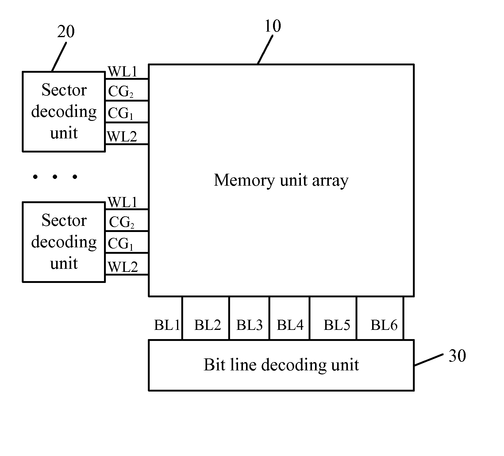
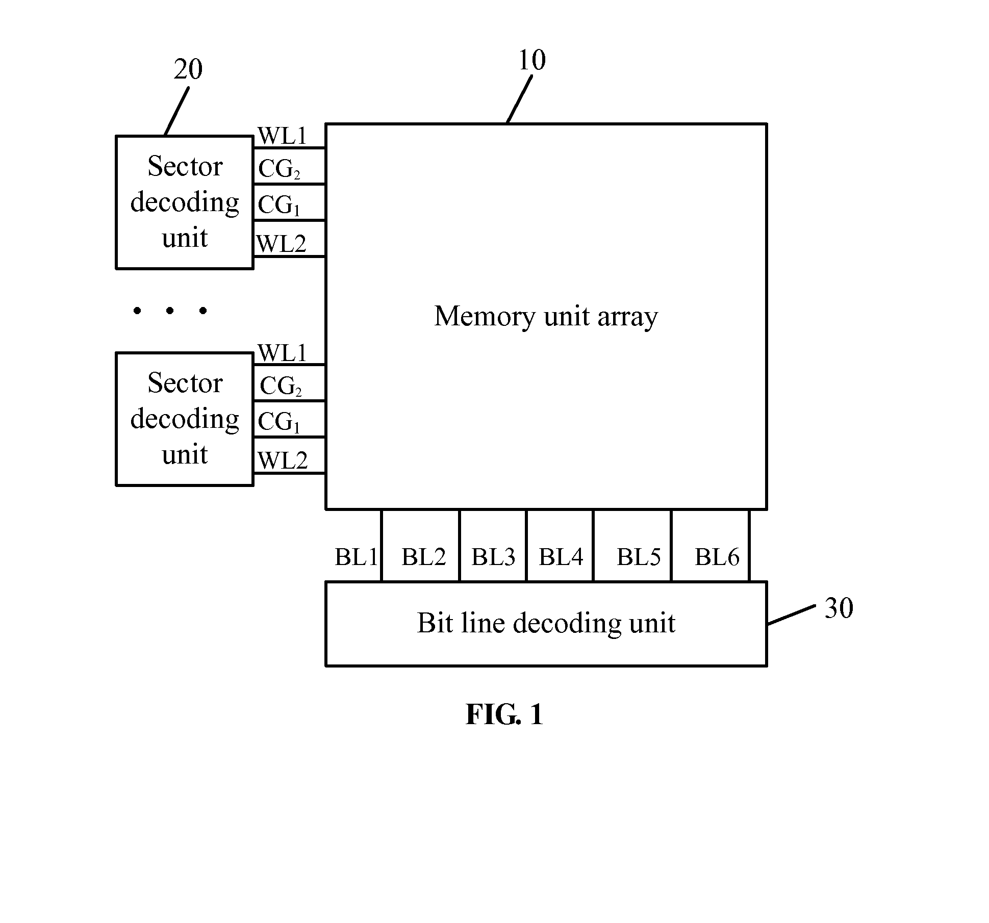
[0024]In conventional techniques, memory densities of flash memory devices are normally increased by changing structures of flash memory unit therein, which may increase processing complexity and manufacturing costs. A memory circuit is provided according to embodiments of the present disclosure. The memory may include a plurality of sectors. Each sector may include at least two parallel rows of memory units, and each memory unit may include a first bit unit and a second bit unit. Each row of memory units may correspond to a first control line controlling the first bit units, a second control line controlling the second bit units, and a word line in parallel with the first and second control lines. A plurality of bit lines are distributed in the memory circuit, which are perpendicular with the word lines. In one sector, at least two neighboring first control lines are connected, and at least two neighboring second control lines are connected.

[0025]Since there are at least two neighb...


PUM


Abstract

A memory circuit is provided, including: a plurality of sectors, where each sector includes at least two parallel rows of memory units; a first control line, a second control line and a word line corresponding to each row of memory units, where at least two of the first control lines which are in the same sector and neighboring with each other are connected, and at least two of the second control lines which are in the same sector and neighboring with each other are connected; and a plurality of bit lines perpendicular with the word lines. The number of the first and second control lines may be reduced, so decoding units which control the control lines may occupy less chip areas, thereby reducing chip areas occupied by the memory circuit.

Description

CROSS REFERENCE TO RELATED APPLICATIONS[0001]The present application claims priority to Chinese Patent Application No. 201210473174.0, filed on Nov. 20, 2012 and entitled “FLASH MEMORY CIRCUIT”, the entire disclosure of which is incorporated herein by reference.FIELD OF THE DISCLOSURE[0002]The present disclosure generally relates to semiconductor technology, and more particularly, to a flash memory circuit with shared control lines.BACKGROUND OF THE DISCLOSURE[0003]Flash memory, attributing to its convenience, high memory density and ideal reliability, has been a research hotspot in non-violate storage devices. Currently, development of flash memory is promoted by motivation of chasing higher memory density. However, due to structure limitation, memory densities of conventional flash memories may no longer be increased by simply shrinking the device dimensions.[0004]Generally, flash memory devices can be classified into two types: gate-split flash memories and stacked flash memories...

Claims


Application Information

Patent Timeline
IPC IPC(8): G11C16/08
CPCG11C16/08G11C16/0441
Inventor GU, JING
Owner SHANGHAI HUAHONG GRACE SEMICON MFG CORP
Why Eureka
Try Eureka