Corner specific normalization of static timing analysis

a static timing analysis and corner specific technology, applied in the field of integrated circuit (ic) design, can solve the problems of large device switching delay, large delay, and inability to predict circuit behavior, so as to avoid inefficient circuit solutions or cost greater design effor

Inactive Publication Date: 2014-05-29
GLOBALFOUNDRIES INC
View PDF3 Cites 16 Cited by
  • Summary
  • Abstract
  • Description
  • Claims
  • Application Information

AI Technical Summary

Benefits of technology

[0019]In another aspect, an embodiment normalizes the slacks, providing an insight into the degree of difficulty of required fixes for the slack across corners. Given multiple analyses, in one embodiment, the method achieves fixing slacks in a correct order (across corners and paths), and avoids inefficient circuit solutions or cost greater design effort than necessary.

Problems solved by technology

A timing analysis at a design corner validates the circuit functionality at that corner, but cannot predict circuit behavior if any of the parameters changes (at a different corner).
While two paths leading to a test can have similar delays at a given corner, the delays may be widely disparate at another corner if the two paths are constituted of disparate circuit elements.
However, this behavior is sub-optimal if the design effort to fix the tested slack for a given point differs amongst the various corners and is worse for the corner with lowest magnitude slacks.
Given that the device delays are larger at the Low corner (lower voltage leads to smaller circuit currents that result in slower signal transitions, thereby causing larger device switching delays), the slacks are commensurately more negative.
Given multiple corner analyses and slacks that vary by path across corners, fixing path slacks in the wrong order may drive inefficient circuit solutions or cost greater design effort than is necessary.
Design-automation tools take a brute-force approach, fixing fails directly as reported by the timing analysis tool, beginning with the worst absolute magnitude fail.

Method used


Image

  • Corner specific normalization of static timing analysis
  • Corner specific normalization of static timing analysis
  • Corner specific normalization of static timing analysis

Examples


Embodiment Construction

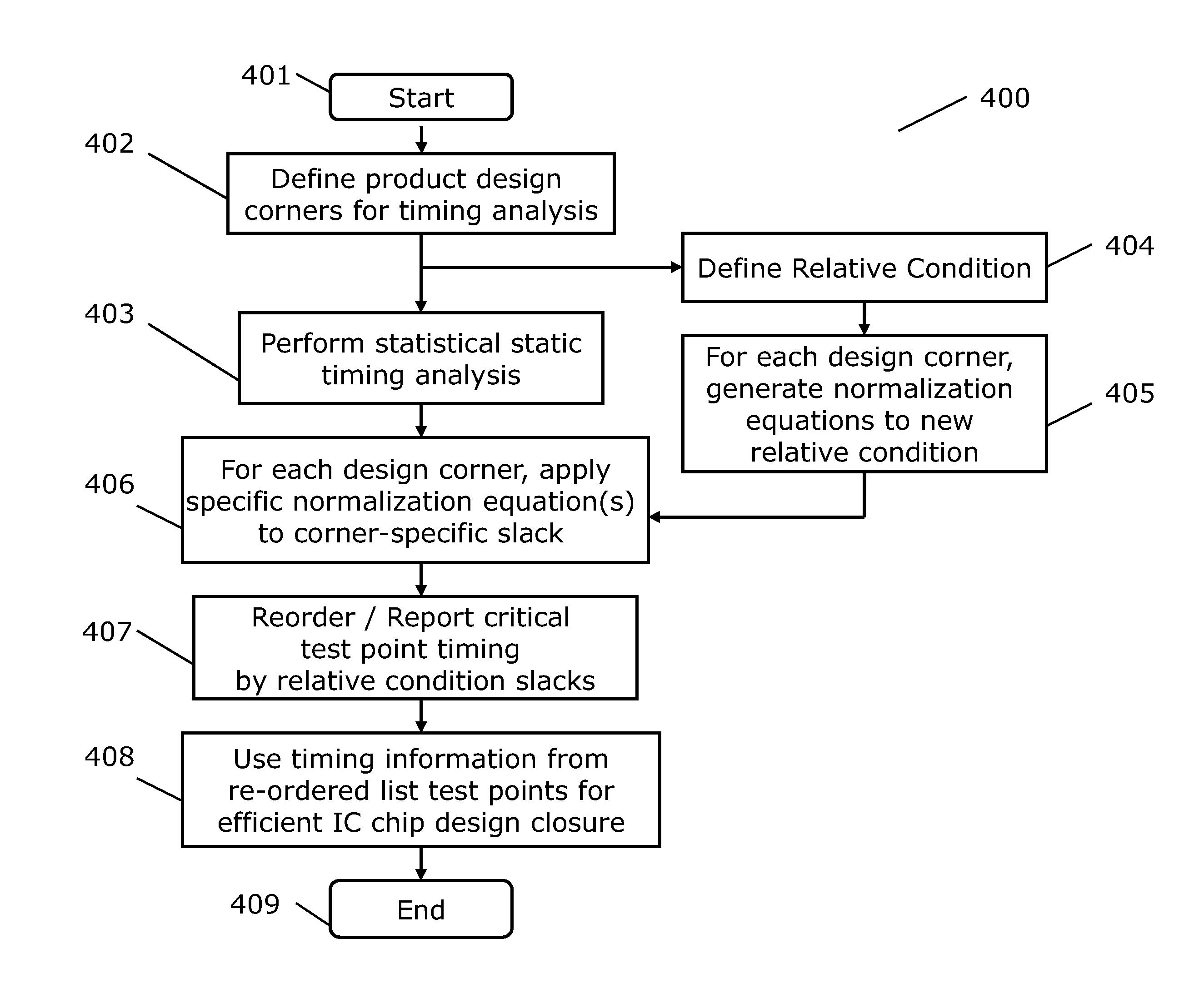
[0022]The present invention and the various features and advantageous details thereof are explained more fully with reference to the non-limiting embodiments that are illustrated in the accompanying drawings and detailed in the following description. Descriptions of well-known components and processing techniques are omitted so as to not unnecessarily obscure the present invention in detail.

[0023]Referring to FIG. 4, a flow diagram illustrates an embodiment of method labeled 400 for timing analysis of a given circuit / chip design with alternate normalization.

[0024]The method 400 is initialized in step 401. The design, timing models, and timing assertions are read. In step 402, design corners are defined. Typically, timing analysis results (including slacks) will be validated at these corners. In an embodiment, two design corners, termed Low and High are selected, representing two different voltage conditions. Across the two voltage conditions, the circuit device delays are substantia...


PUM


Abstract

A method and a system for expressing results of a timing analysis of an integrated circuit (IC) chip design as relative values to drive efficient chip design closure include: using a computer, performing the timing analysis to compute timing results of the chip design across at least two design corners; applying corner specific normalization equations to the timing analysis results from each of the at least two corners to obtain normalized timing results; and using the timing results ordered and filtered by the normalized timing results of the IC chip design for the design closure prior to chip manufacture. The slacks are normalized to provide insight into the degree of difficulty of the required fixes for that slack across corners. Given multiple analyses, the slacks are fixed in a correct order across corners and paths, avoiding inefficient circuit solutions or cost greater design effort.

Description

FIELD OF THE INVENTION[0001]The present invention relates to integrated circuit (IC) design and the application of Electronic Design Automation (EDA) based on static timing analysis (STA) tools to circuits, and more particularly, it relates to ordering test points and corners (conditions) when applying an STA across multiple timing analysis design corners for efficient chip design closure.BACKGROUND[0002]Conventional circuit Static Timing Analysis (STA) is used to validate and compute signal propagation and arrival times at multiple points in a given circuit. A path in a circuit denotes a topologically ordered set of connected circuit components that allow electrical signal propagation. STA computes the signal arrival times along points in a path, and thus can be used to compute signal propagation times or delays of any path. FIG. 1 illustrates a block diagram depicting two paths in a circuit that have a timing constraint between their respective end (or sink) test points. Path 1 st...

Claims


Application Information

Patent Timeline
Patent Type & Authority Applications(United States)
IPC IPC(8): G06F17/50
CPCG06F30/3312G06F2119/12
Inventor FLUHR, ERIC J.SHUMA, STEPHEN G.SINHA, DEBJITWOOD, MICHAEL H.
Owner GLOBALFOUNDRIES INC
Why Eureka
Try Eureka