Method for Producing an Optoelectronic Semiconductor Component and Such a Semiconductor Component

Inactive Publication Date: 2014-06-05
OSRAM OPTO SEMICON GMBH & CO OHG
View PDF6 Cites 8 Cited by
  • Summary
  • Abstract
  • Description
  • Claims
  • Application Information

AI Technical Summary

Benefits of technology

[0004]Embodiments of the present invention provide a production method that avoids the above-stated disadvantages, resulting advanta

Problems solved by technology

Such a mechanically unsupported region for separating the unilateral electrical contacts disadvantageously lead

Method used


Image

  • Method for Producing an Optoelectronic Semiconductor Component and Such a Semiconductor Component
  • Method for Producing an Optoelectronic Semiconductor Component and Such a Semiconductor Component
  • Method for Producing an Optoelectronic Semiconductor Component and Such a Semiconductor Component

Examples


Example

[0052]In the figures, identical or identically acting components may in each case be provided with the same reference numerals. The components illustrated and their size ratios to one another should not be viewed as being to scale. Rather, individual elements such as, for example, layers, structures, components and regions are shown exaggeratedly thick or large for greater ease of depiction and / or better comprehension.

DETAILED DESCRIPTION OF ILLUSTRATIVE EMBODIMENTS

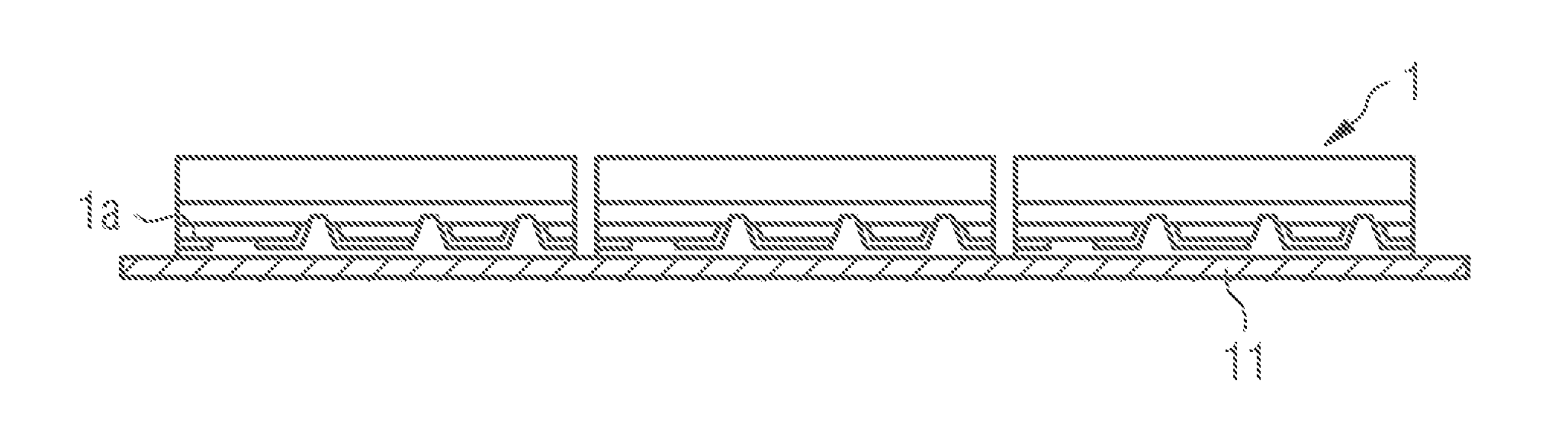
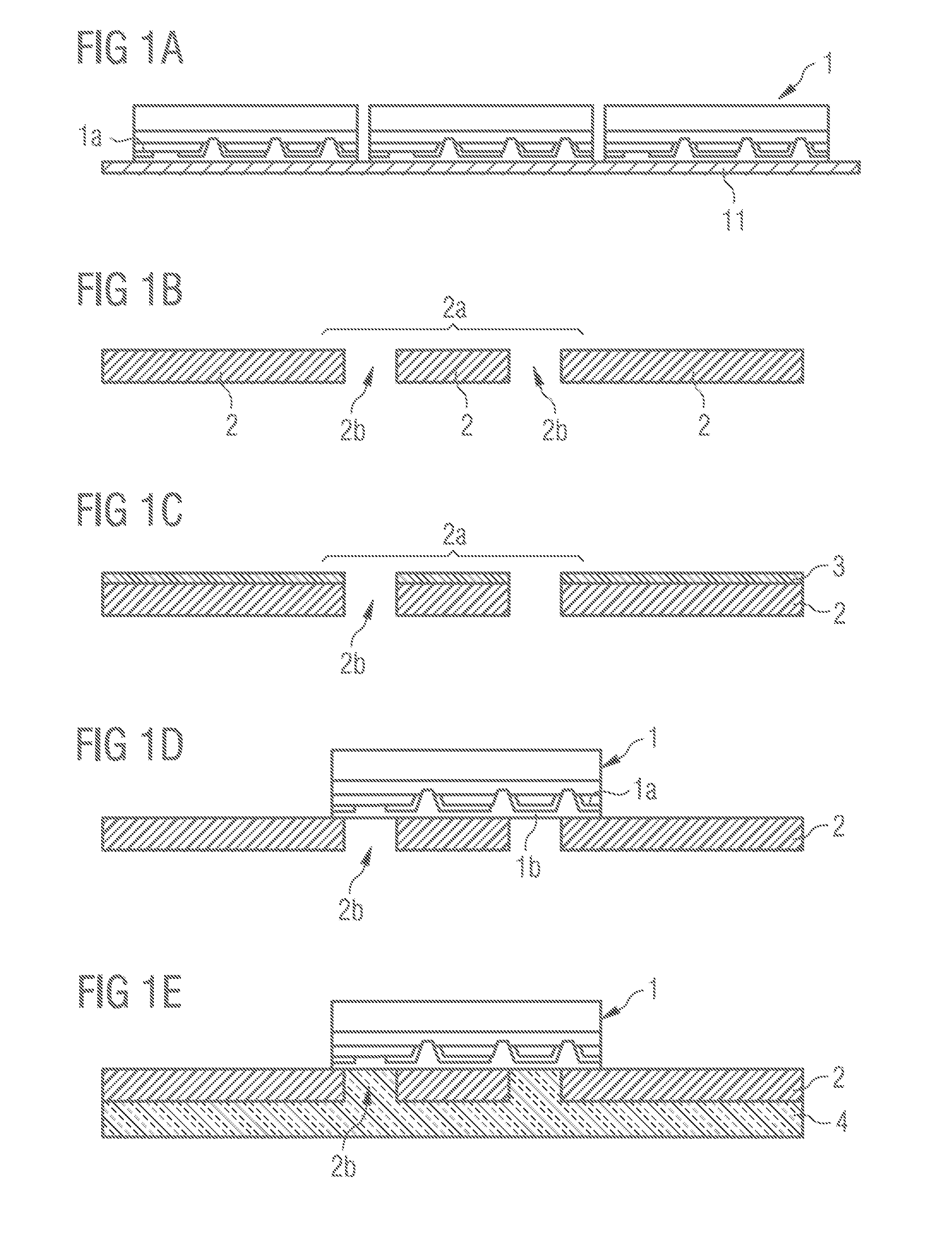
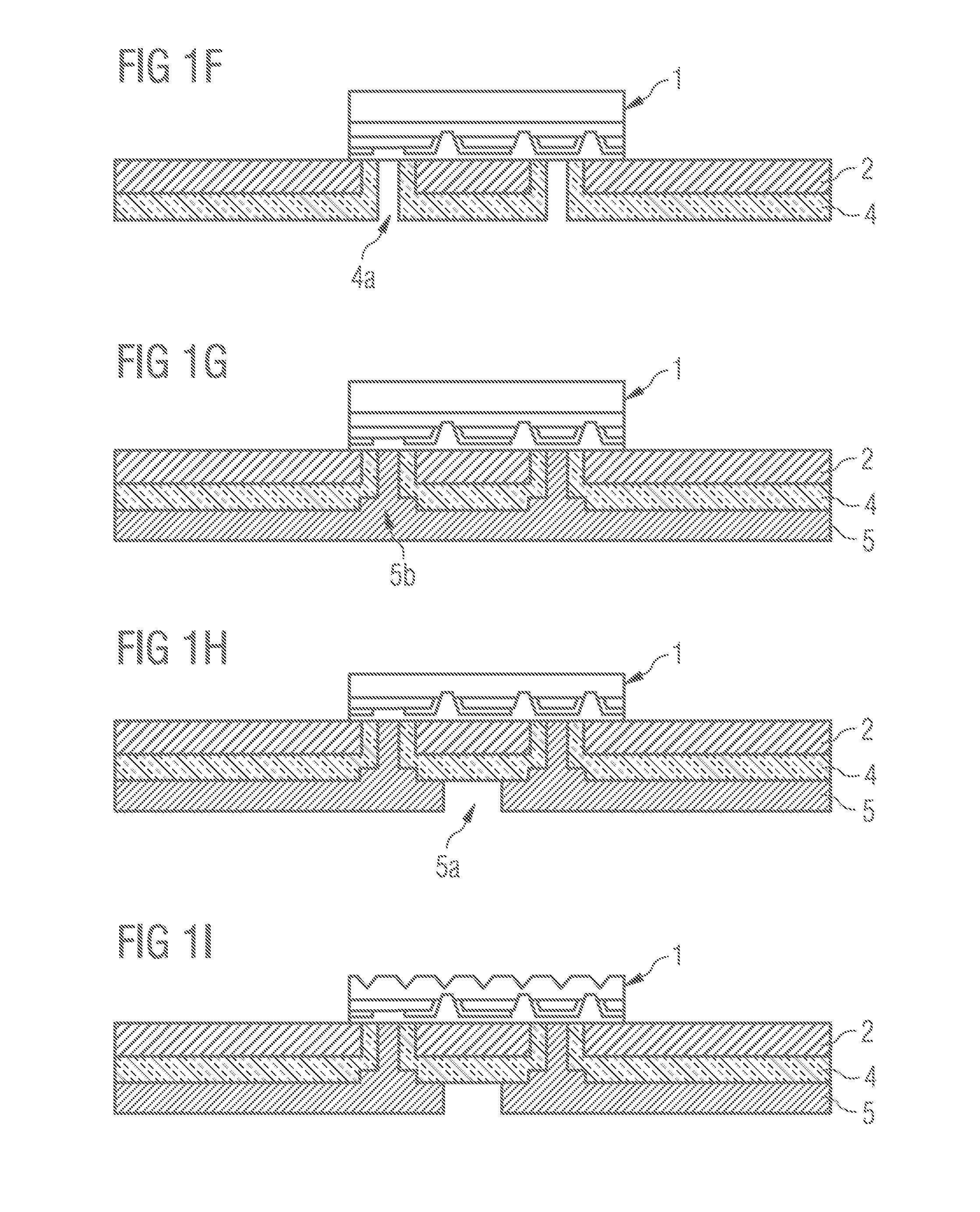
[0053]FIGS. 1A to 1K in each case show cross-sections of a semiconductor component in process of being produced. In FIG. 1A a substrate 11 is provided, on which a plurality of semiconductor chips 1 are arranged. The substrate 11 preferably takes the form of a foil. The semiconductor chips 1 each comprise an active layer 1a suitable for generating radiation. The semiconductor chips 1 are LEDs, for example, and preferably exhibit unilateral contacting, so meaning that the semiconductor chips 1 each have both contact regions...


PUM


Abstract

A method for producing a semiconductor component is disclosed. A carrier substrate includes a mounting region and an opening, which is formed in the mounting region of the carrier substrate. After mounting a semiconductor chip, an electrically insulating layer is applied to the carrier substrate in such a way that the electrically insulating layer completely fills the first opening in the carrier substrate. A second opening is formed in the electrically insulating layer. An electrically conductive layer is then applied to the electrically insulating layer in such a way that the second opening is filled with the electrically conductive layer in the form of a via. A semiconductor component produced in this way is also provided.

Description

[0001]This patent application is a national phase filing under section 371 of PCT / EP2012 / 058921, filed May 14, 2012, which claims the priority of German patent application 10 2011 103 412.2, filed Jun. 6, 2011, each of which is incorporated herein by reference in its entirety.TECHNICAL FIELD[0002]The invention relates to a method for producing an optoelectronic component comprising a carrier substrate and a semiconductor chip. The present invention further relates to such an optoelectronic semiconductor component.BACKGROUND[0003]When producing semiconductor components with thin semiconductor chips, which inter alia comprise unilateral electrical contacting, precise adjustment processes are necessary in order to mount the semiconductor chip on carrier substrates. For example, in the case of a semiconductor chip which comprises annular insulation between the p- and n-contact regions of the semiconductor chip, the annular region is free-standing and not supported mechanically by the ca...

Claims


Application Information

Patent Timeline
IPC IPC(8): H01L31/0236H01L33/48H01L31/18H01L33/22
CPCH01L31/0236H01L33/48H01L33/22H01L31/18H01L24/18H01L24/96H01L33/62H01L33/486H01L25/0753H01L2224/04105H01L2224/92144H01L2933/0066H01L2933/0033H01L24/19H01L2224/24137H01L2924/15787H01L2924/12042H01L2924/12036H01L24/82H01L2924/10158H01L24/24H01L2924/00
Inventor HERRMANN, SIEGFRIED
Owner OSRAM OPTO SEMICON GMBH & CO OHG
Why Eureka
Try Eureka