Optical modulation device and bias voltage control method

a technology of optical modulation device and bias voltage control, which is applied in the direction of optics, digital transmission, instruments, etc., can solve the problem of relativly difficult to detect a drift occurring in vsub>bias3/sub>, and achieve the effect of maximizing or minimizing an optical power

Active Publication Date: 2014-06-05
NIPPON TELEGRAPH & TELEPHONE CORP
View PDF10 Cites 21 Cited by
  • Summary
  • Abstract
  • Description
  • Claims
  • Application Information

AI Technical Summary

Benefits of technology

[0137]According to the present disclosure, it is possible to provide a technique for appropriately selecting wheth

Problems solved by technology

Therefore, it is relatively difficult

Method used


Image

  • Optical modulation device and bias voltage control method
  • Optical modulation device and bias voltage control method
  • Optical modulation device and bias voltage control method

Examples


first embodiment

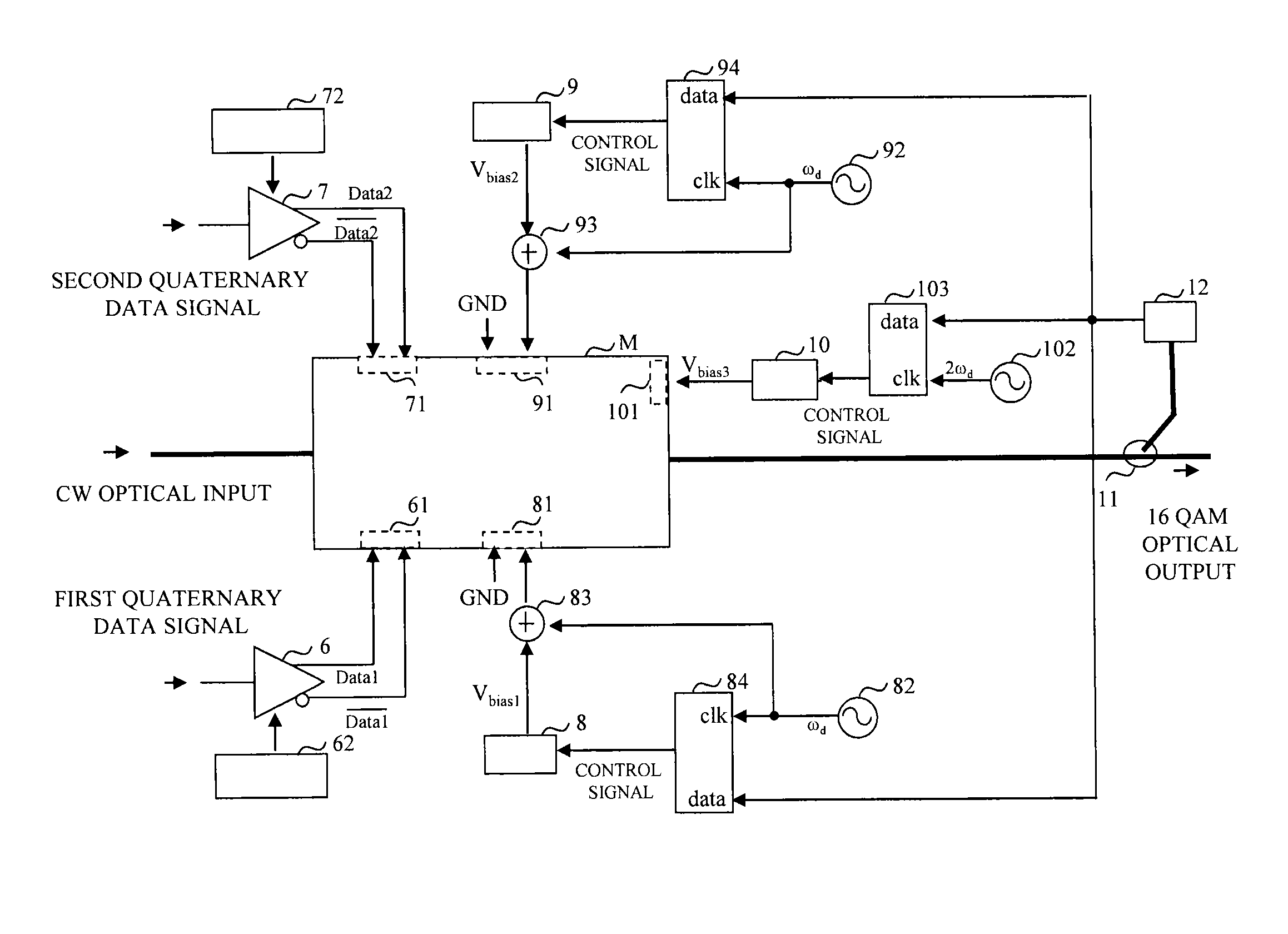
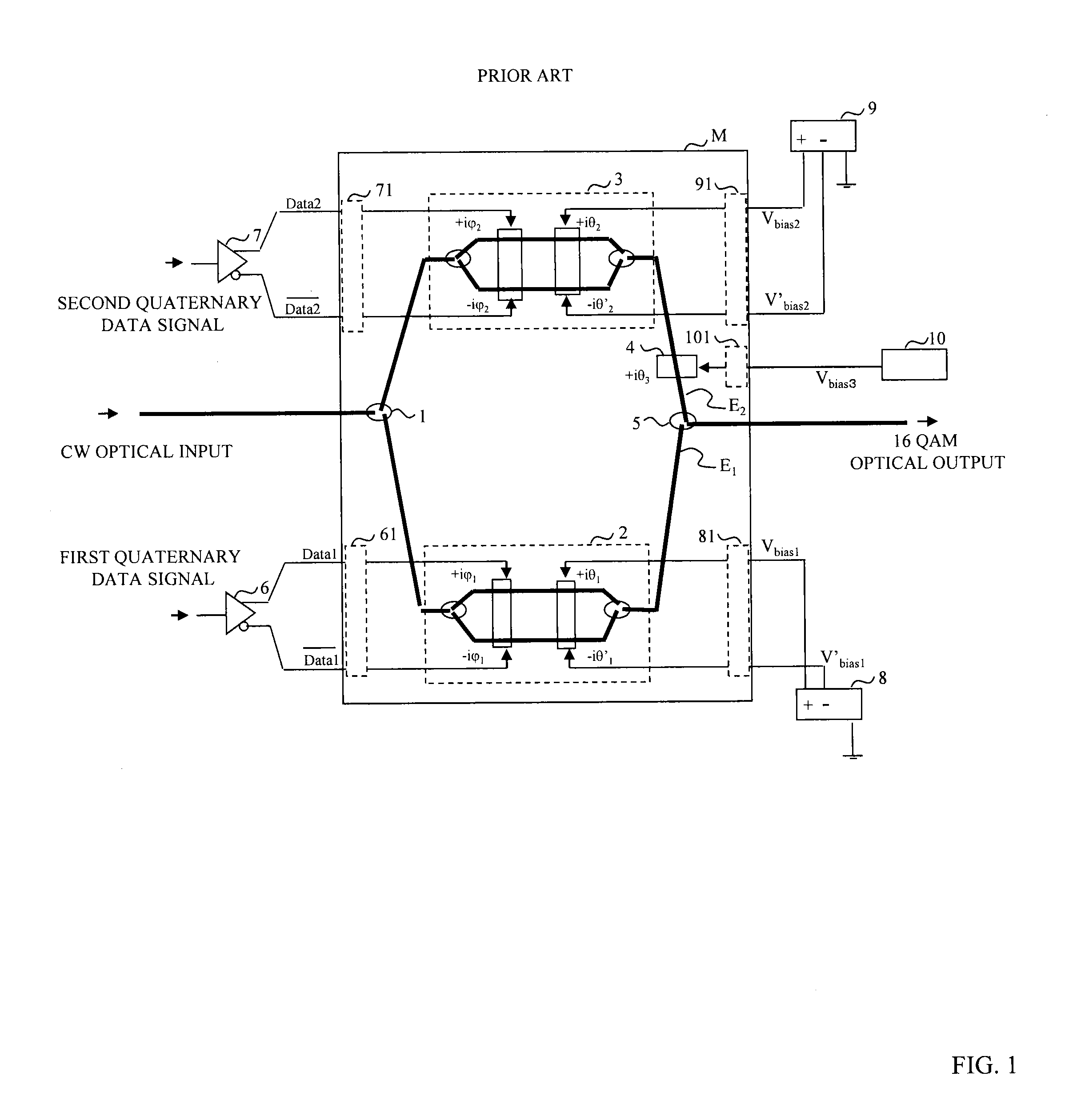
[0175]FIG. 10 shows the configuration of an optical modulation device according to a first embodiment. In the dual drive type IQ optical modulator M, the differential drive signals Data1 and Data1 and Data2 and Data2 output from the first and second driving amplifiers 6 and 7 are applied to the first and second driving electrodes 61 and 71. The first and second quaternary data signals are input to the first and second driving amplifiers 6 and 7 and the output amplitudes of the signals are adjusted by the first and second amplitude adjustment units 62 and 72. In the first embodiment, pre-emphasis is not used, and the four signal levels V0, V1, −V1, and −V0 of the differential signals added to the first and second driving electrodes 61 and 71 are set at even intervals. In other words, (Data1- Data1) and (Data2- Data2) have the four values V0, V1, −V1, and −V0, and |V0−V1|=|V1−(−V1)| is established.

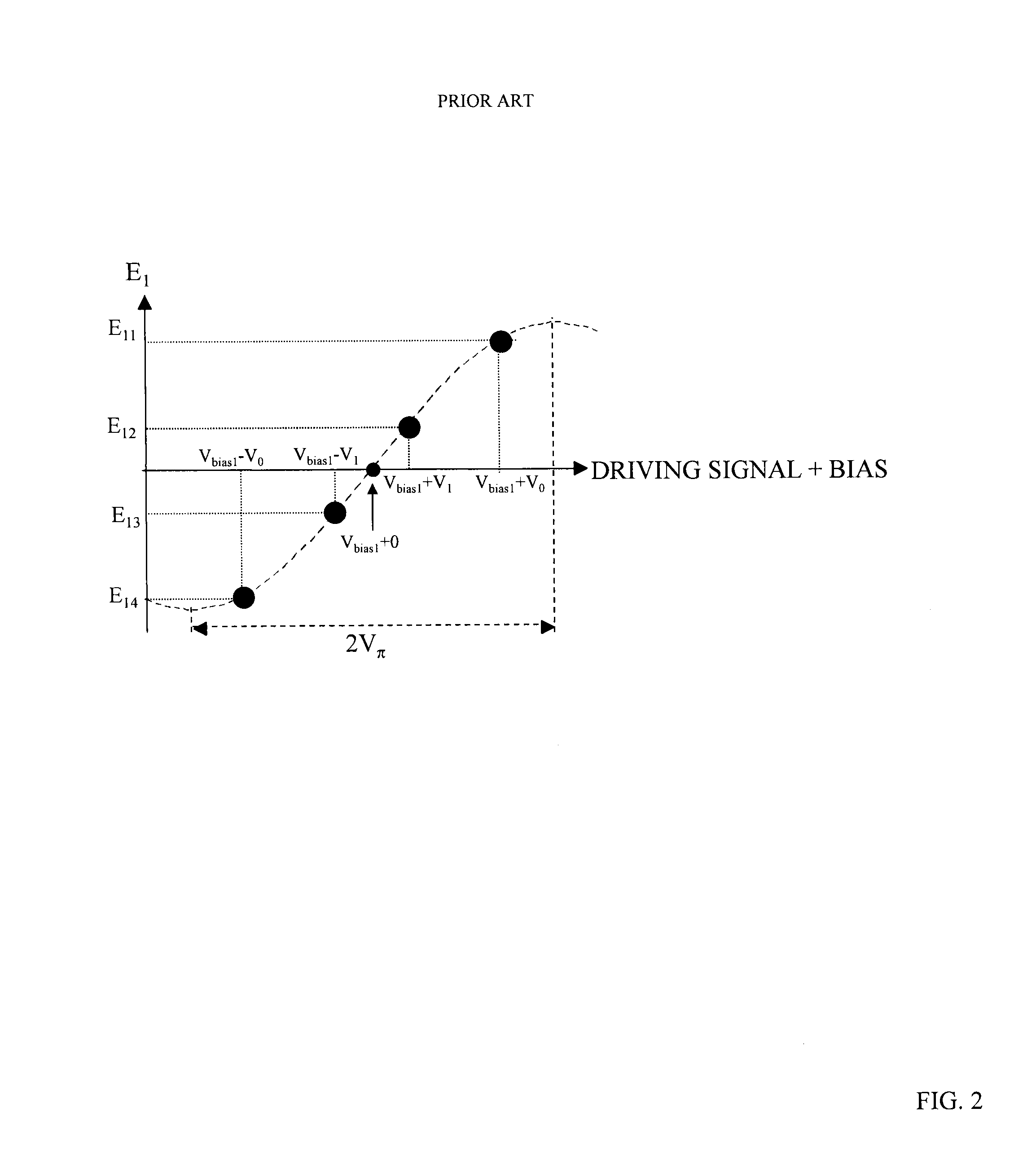
[0176]As a first specific example, it is assumed that the interval between the four leve...

second embodiment

[0187]FIG. 11 shows the configuration of an optical modulation device according to a second embodiment. As the difference between the first and second embodiments, pre-emphasis is used to set the values of the electric fields E11, E12, E13, and E14 of the four types of light output from the first optical modulation unit 2 at even intervals and set the values of the electric fields E21, E22, E23, and E24 of the four types of light output from the second optical modulation unit 3 at even intervals. In other words, Equation 18 is established.

E11=E21=sin(V0 / Vπ×π / 2)

E12E22=sin(V1 / Vπ×π / 2)

E13E23=sin(−V1 / Vπ×π / 2)

E14E24=sin(−V0 / Vπ×π / 2)

|sin(V0 / Vπ×π / 2)−sin(V1 / Vπ×π / 2)|=2|sin(V1 / Vπ×π / 2)|  (Equation 18)

[0188]Required V0 and V1 are obtained when the first and second quaternary data signals are input to the first and second pre-emphasis units 63 and 73, respectively. The control of Vbias1 to Vbias3 is performed in the same manner as the first embodiment.

[0189]As a first specific example, it is assume...

third embodiment

[0191]FIG. 12 shows the configuration of an optical modulation device according to a third embodiment. The third embodiment is different from the first embodiment in two points.

[0192]A first different point is that this embodiment uses a single driving type IQ optical modulator M instead of a dual driving type IQ optical modulator M. Each of the first and second driving amplifiers 6 and 7 performs a single-phase output, and their outputs Data1 and Data2 have the four signal levels V0, V1, −V1, and −V0 relative to the ground level. Although twice the output amplitude of the first embodiment is required, there is an advantage in that the mounting area of the IQ optical modulator M can be reduced.

[0193]A second different point is that the first and second bias power supplies 8 and 9 perform a single-phase output, their DC voltages are converted into differential signals by the first and second dithering amplifiers 85 and 95 after having the outputs of the first and second oscillators 8...


PUM


Abstract

An optical modulation device including: bias power supplies that output a signal having a bias voltage corresponding to the null point of an optical modulation unit to the optical modulation unit; and synchronous detection circuits that determine whether an intensity of a QAM signal at a drift non-occurrence time where no drift occurs in the bias voltage becomes larger or smaller than the intensity of the QAM signal at a drift occurrence time where a drift occurs in the bias voltage, adjust the bias voltage to maximize the intensity of the QAM signal when determining that the intensity of the QAM signal at the drift non-occurrence time becomes larger than the intensity of the QAM signal at the drift occurrence time, and adjust the bias voltage to minimize the intensity of the QAM signal when determining that the intensity of the QAM signal at the drift non-occurrence time becomes smaller than the intensity of the QAM signal at the drift occurrence time.

Description

BACKGROUND[0001]1. Field of the Disclosure[0002]The present disclosure relates to an automatic bias voltage control of an optical modulation device for use in multi Quadrature Amplitude Modulation (QAM). In particular, the present disclosure is suitable for the automatic bias voltage control of an optical modulation device that sends a quaternary or larger value QAM signal.[0003]2. Discussion of the Background Art[0004]As a transmission code for use in an optical transmission system, a QAM signal, capable of sending a large amount of optical signals at a low symbol rate has been paid attention. The simplest QAM is quaternary QAM and called Quadrature Phase Shift Keying (QPSK). The present disclosure is applicable to any multi-QAM modulators including QPSK, however for simplicity, a description will be mainly given of a 16 QAM system in the present disclosure. Here, some symbols have a bar placed on characters in figures, however placed before the characters indicates that the symbol...

Claims


Application Information

Patent Timeline
IPC IPC(8): G02F1/01
CPCG02F1/0123G02F1/21G02F1/212H04B10/5053H04B10/50575H04B10/541H04L27/3411H04L27/364G02B6/28H04B10/50595H04B10/548
Inventor KAWAKAMI, HIROTOYOSHIDA, EIJIMIYAMOTO, YUTAKA
Owner NIPPON TELEGRAPH & TELEPHONE CORP
Why Eureka
Try Eureka