
Magnetoresistive sensor integrated in a chip for detecting magnetic fields perpendicular to the chip and manufacturing process thereof

a technology of magnetic field and integrated chip, which is applied in the direction of magnetic measurement, special surfaces, instruments, etc., can solve the problems of complex assembly operation, difficult third-direction detection, and high cost of end devices

Active Publication Date: 2014-06-12
STMICROELECTRONICS INT NV
View PDF2 Cites 24 Cited by
  • Summary
  • Abstract
  • Description
  • Claims
  • Application Information

AI Technical Summary

Benefits of technology

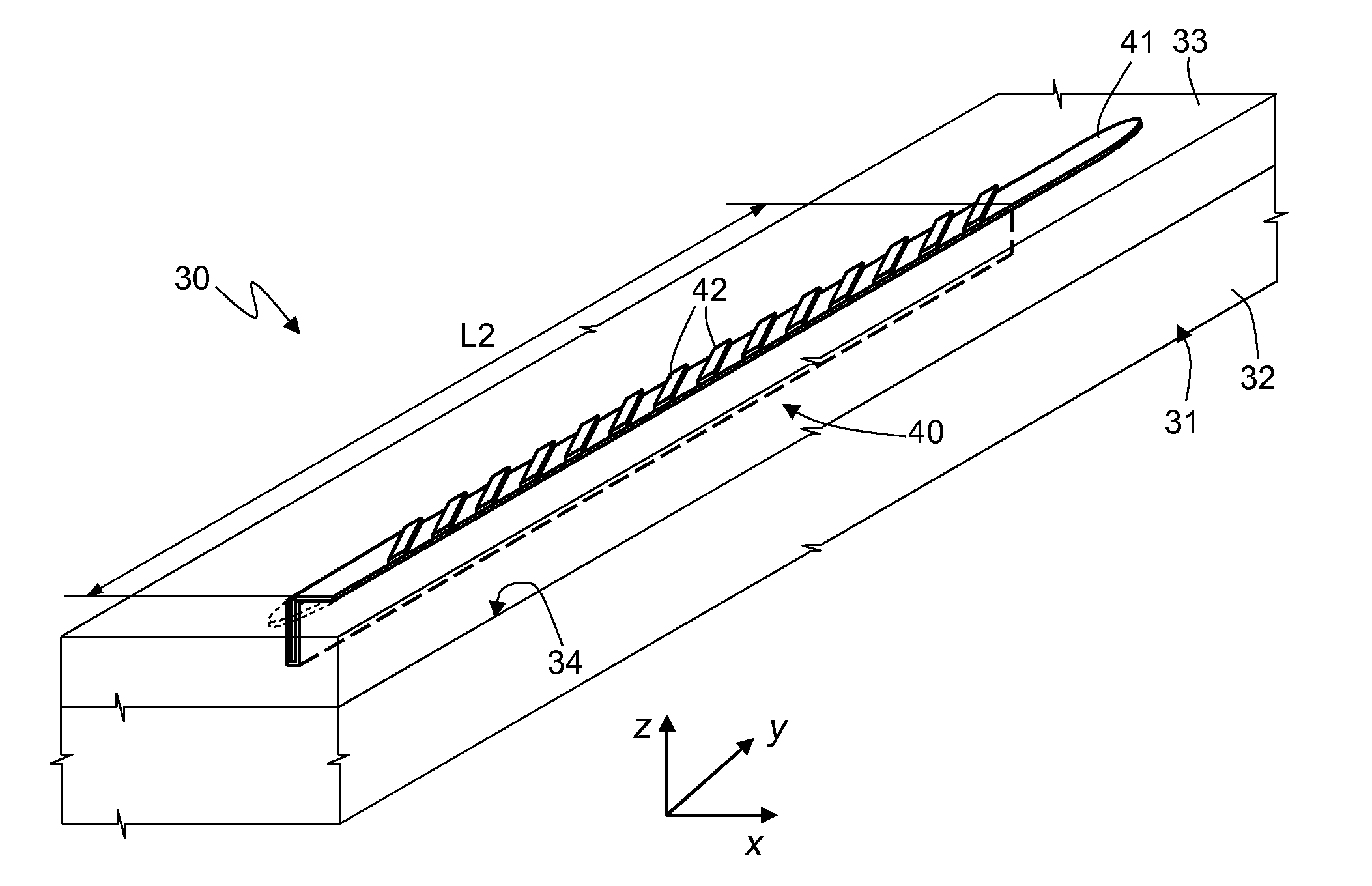
The present patent describes a magnetoresistive sensor that can detect magnetic fields perpendicular to a chip. The sensor includes a chip with a substrate and an insulating region, and a first magnetoresistor and a first concentrator, which are formed in the chip. The chip is designed to provide a more accurate and precise detection of magnetic fields, which can be useful in various applications such as magnetic field mapping or navigation. The manufacturing process of the sensor is also provided.

Problems solved by technology

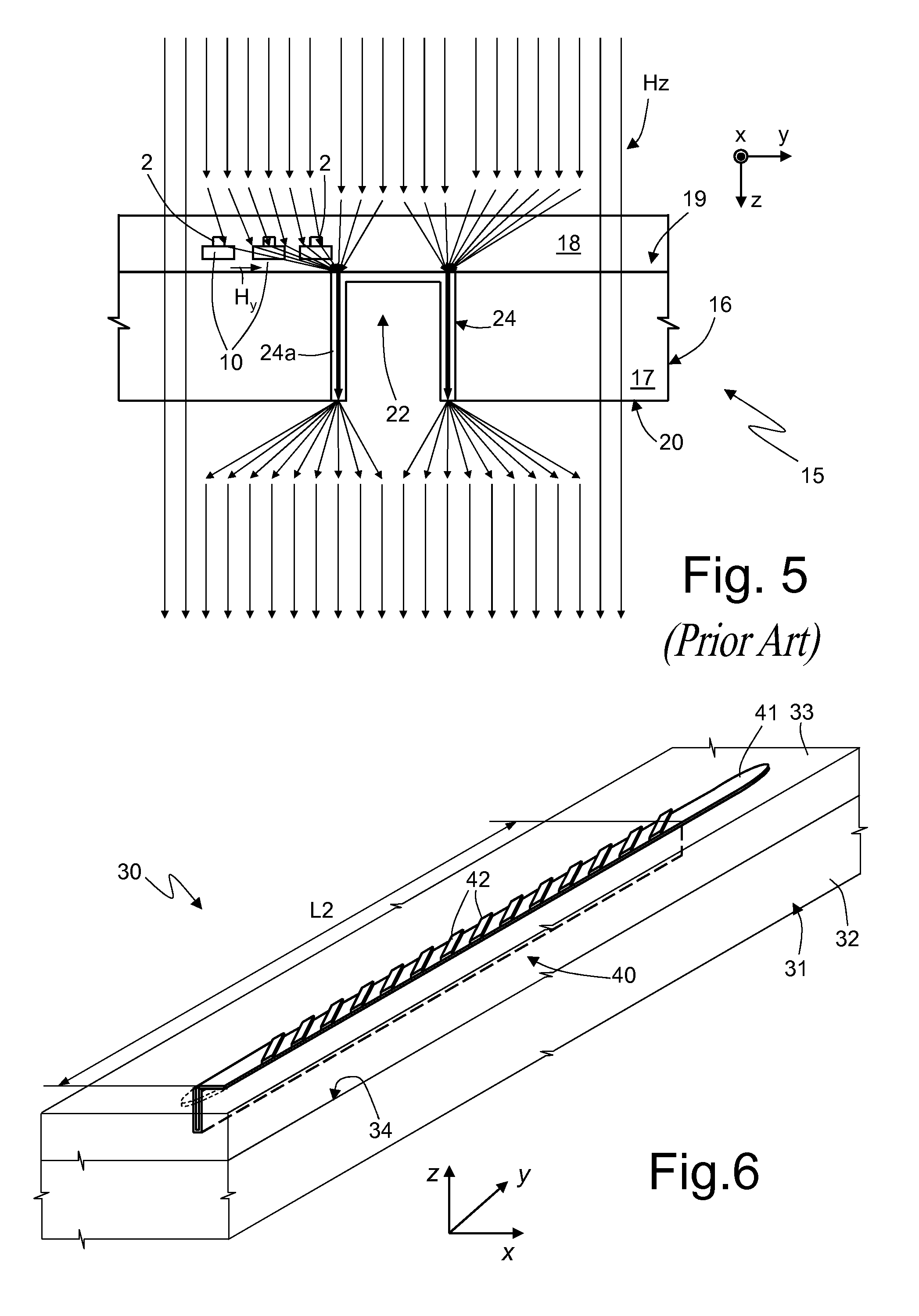
Whereas creation of a sensor sensitive to fields oriented in two directions does not create difficulties, since they lie in a same plane, third direction detection is difficult, since prior art production methods construct a third sensor arranged in a plane perpendicular to the first two sensors.
Since current technologies do not enable industrial production at acceptable costs of vertical magnetoresistors, sensitive to the axis Z, in some compasses the sensor Z is obtained in planar form, as sensors X and Y, and the corresponding chip is attached on a base or frame in a vertical position, perpendicular to the sensors X and Y. However, in this case, the assembly operations are complex, and the end device is costly.
Moreover, the packaged device has an excessive volume (in particular height), which does not enable use thereof in small apparatuses.
This phenomenon causes an undesirable reduction and above all a sensitivity variation between sensors formed in different semiconductor wafers or even between sensors formed in a same wafer.

Method used


Image

  • Magnetoresistive sensor integrated in a chip for detecting magnetic fields perpendicular to the chip and manufacturing process thereof
  • Magnetoresistive sensor integrated in a chip for detecting magnetic fields perpendicular to the chip and manufacturing process thereof
  • Magnetoresistive sensor integrated in a chip for detecting magnetic fields perpendicular to the chip and manufacturing process thereof

Examples


Embodiment Construction

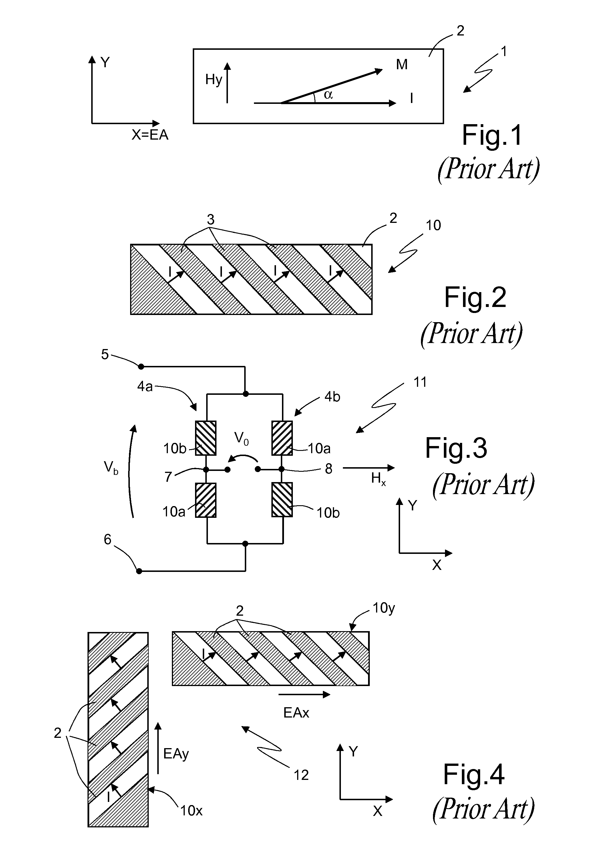
[0004]In the following description, particular reference will be made to an anisotropic-magnetoresistor (AMR) sensor, without, however, being limited thereto, and the disclosure may be applied also to other types of magnetoresistive sensors, such as the giant-magnetoresistor (GMR) sensor and the tunneling-magnetoresistor (TMR) sensor and other integrated magnetic-field sensors that are sensitive to magnetic fields parallel to the chip integrating them.

[0005]As is known, magnetoresistive sensors exploit the capacity of appropriate ferromagnetic materials (referred to as “magnetoresistive materials”, for example the material known as “permalloy” which is an NiFe alloy) to modify their own resistance in presence of an external magnetic field.

[0006]Currently, magnetoresistive sensors are obtained from strips of magnetoresistive material. In case of anisotropic magnetoresistive sensors, during the manufacturing process, the strip of magnetoresistive material may be subjected to an extern...


PUM


Abstract

An integrated magnetoresistive sensor, formed in a chip including a substrate having a surface and an insulating region covering the surface of the substrate. A magnetoresistor, of a first ferromagnetic material, is formed in the insulating region and has a sensitivity plane parallel to the surface. A concentrator of a second ferromagnetic material is formed in the substrate and has at least one arm extending in a transverse direction to the sensitivity plane. The arm has one end in contact with the magnetoresistor.

Description

BACKGROUND[0001]1. Technical Field[0002]The present disclosure relates to a magnetoresistive sensor integrated in a chip for detecting magnetic fields perpendicular to the chip, as well as to its manufacturing process.[0003]2. Detailed Description[0004]In the following description, particular reference will be made to an anisotropic-magnetoresistor (AMR) sensor, without, however, being limited thereto, and the disclosure may be applied also to other types of magnetoresistive sensors, such as the giant-magnetoresistor (GMR) sensor and the tunneling-magnetoresistor (TMR) sensor and other integrated magnetic-field sensors that are sensitive to magnetic fields parallel to the chip integrating them.[0005]As is known, magnetoresistive sensors exploit the capacity of appropriate ferromagnetic materials (referred to as “magnetoresistive materials”, for example the material known as “permalloy” which is an NiFe alloy) to modify their own resistance in presence of an external magnetic field.[...

Claims


Application Information

Patent Timeline
Patent Type & Authority Applications(United States)
IPC IPC(8): G01R33/09G01R33/00
CPCG01R33/0011G01R33/096G01R33/0052G01R33/09
Inventor PACI, DARIOFARALLI, DINOPICCO, ANDREA
Owner STMICROELECTRONICS INT NV
Learn More