Method of producing a single crystal gallium nitride substrate and single crystal gallium nitride substrate

Inactive Publication Date: 2002-03-07
SUMITOMO ELECTRIC IND LTD
View PDF0 Cites 104 Cited by
  • Summary
  • Abstract
  • Description
  • Claims
  • Application Information

AI Technical Summary

Benefits of technology

0163] Unlike the imagined prior art, this invention succeeds in obtaining an effect of reducing dislocations superficially and substantially by slicing an ingot

Problems solved by technology

Lack of natural cleavage compels device makers to cut (dice) mechanically sapphire wafers crosswise and lengthwise into device chips with an application of strong forces.
The dicing process incurs an extra cost and decreases a yield in the production of GaN LEDs.
Uncleavability of GaN crystals subjects GaN/sapphire LDs to other difficulties besides the problems of dicing.
Uncleavable GaN prevents GaN laser diodes from making resonator mirrors by natural cleavage, which invites difficulties on laser oscillation performance and on production cost.
Another difficulty originates from the fact that sapphire is an insulator.
The extra etching, the extra thick film and an extra wirebonding raise the cost by increasing the time of fabrication and the number of steps.
This point incurs an increment of the cost.
The sapphire substrates are suffering from these difficulties.
Silicon carbide, however, has some drawbacks.
Single crystal silicon carbide is highly expensive.
The difficulty of producing SiC single crystals will jeopardize a continual, stable supply of SiC substrates.
The crystalline property of GaN films grown on SiC substrates are still bad at present.
SiC is not deemed to be the suitable material as a substrate of GaN light emission devices.
GaN/SiC LEDs are not brought onto market yet.
Sapphire or silicon carbide as a substrate induces many dislocations and other defects in GaN type films grown thereupon owing to mismatches of lattice constants and thermal expansion coefficients between the upper films and the bottom substrate.
However, in the case of GaN/sapphire LDs which require large current density, experiments clarify the fact that the big dislocation density forbids the on-sapphire GaN type LDs from having a long lifetime.
The big current increases the dislocations and other defects.
The fabrication of the resonator mirror would raise the cost of GaN/sapphire LDs.
The high cost and short lifetime degrade sapphire as a substrate for GaN LDs.
From the reasons, sapphire and silicon carbide are not the most suitable material for the substrates of GaN LDs.
However, crystal growth technology has not been matured for GaN yet.
It is difficult at present to produce gallium nitride single crystals with a large size sufficient for the substrates of GaN LDs.
However, even if it succeeded, the ultrahigh pressure method would synthesize only a small GaN crystal which would be insufficient for the

Method used


Image

  • Method of producing a single crystal gallium nitride substrate and single crystal gallium nitride substrate
  • Method of producing a single crystal gallium nitride substrate and single crystal gallium nitride substrate
  • Method of producing a single crystal gallium nitride substrate and single crystal gallium nitride substrate

Examples


embodiment 1-d

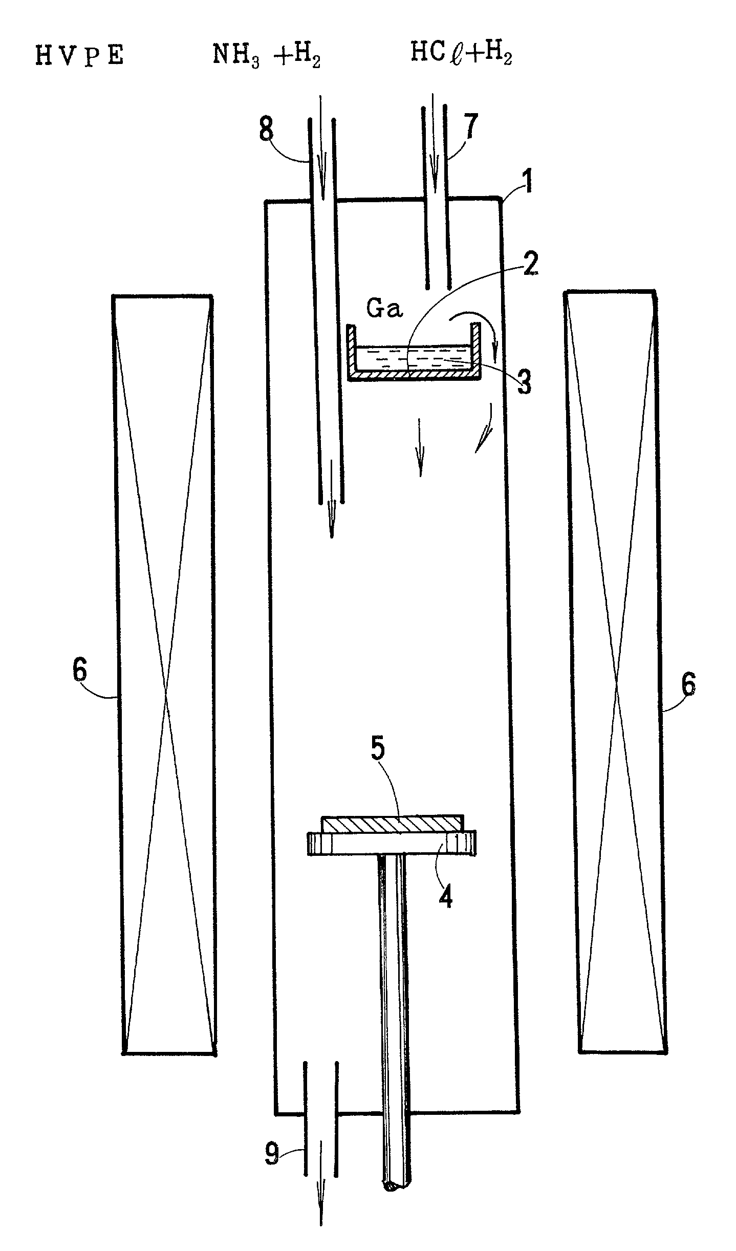
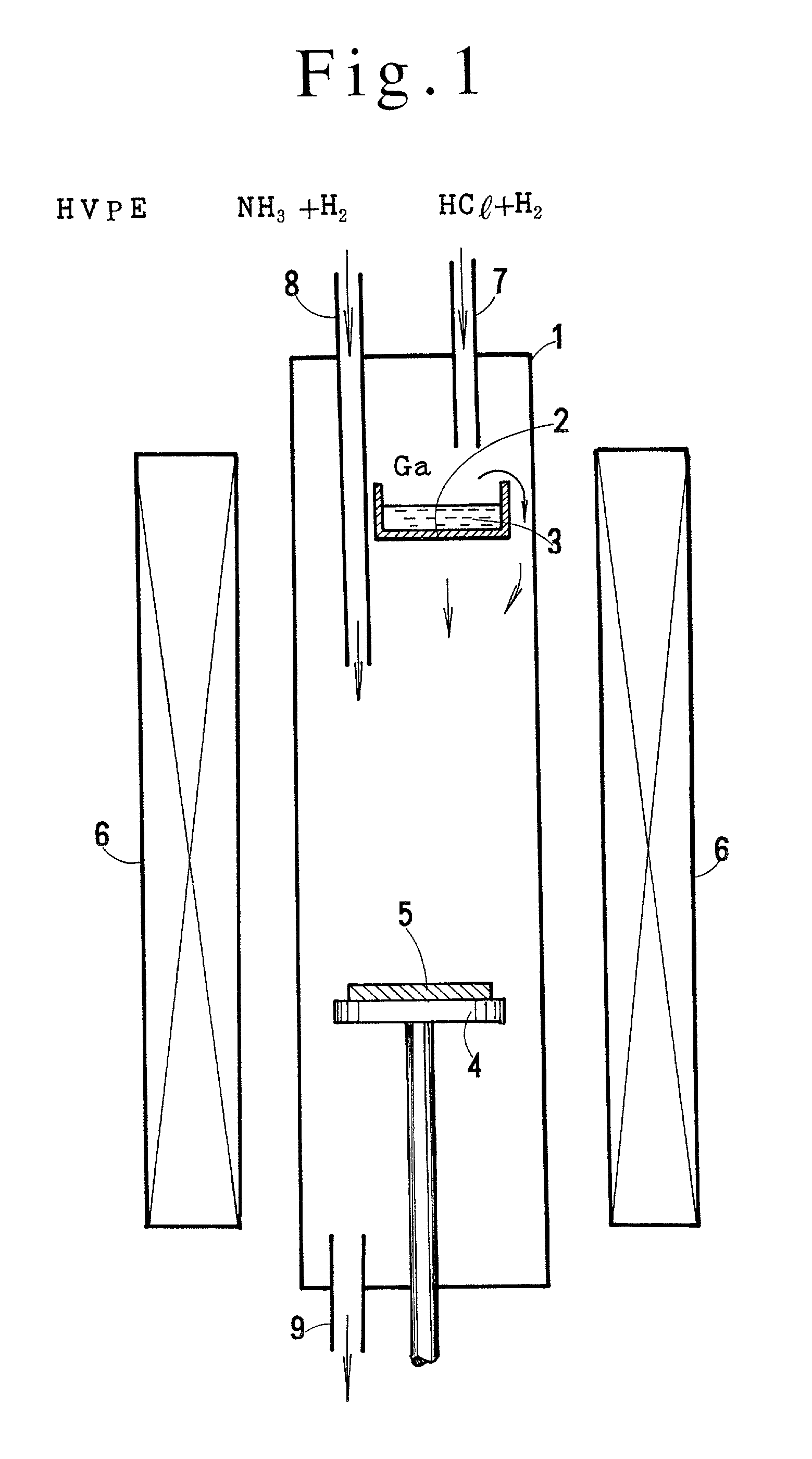
[0319] (EMBODIMENT 1-d) HVPE Apparatus

[0320] The GaAs substrate with the window-carrying mask is laid upon the susceptor 4 in the furnace 1 of the HVPE apparatus as shown in FIG. 1. The HVPE apparatus is designed to be suitable for a long time growth. A GaN freestanding substrate requires a long time growth of GaN.

[0321] The Ga-boat 2 and the susceptor 4 are heated by the heater 6. The Ga is molten in the Ga-boat 2. A mixture of H.sub.2 and HCl gas is supplied to the Ga-melt 3 through the gas inlet 7. Another mixture of H.sub.2 and NH.sub.3 gas is replenished to a space above the susceptor 4 in the furnace 1.

[0322] HCl gas with a carrier H.sub.2 gas is supplied to the Ga-melt heated at about 800.degree. C. Reaction of HCl with Ga makes gallium chloride (GaCl) vapor. The GaCl vapor flows downward near the heated GaAs substrate 5 and reacts with ammonia gas NH.sub.3. The reaction synthesizes GaN. GaN molecules are piled upon the heated GaAs substrate 5. Piling of the GaN makes GaN iso...

embodiment 1-e

[0323] (EMBODIMENT 1-e) Formation of GaN Buffer Layers

[0324] The HVPE apparatus makes about 80 nm thick buffer layers upon the revealed surface of the GaAs substrate within the windows under the condition,

1 Growing temperature about 500.degree. C. (about 773 K) NH.sub.3 gas partial pressure 0.2 atm (20 kPa) HCl gas partial pressure 2 .times. 10.sup.-3 atm (0.2 kPa) Growing time 30 minutes layer thickness 80 nm.

[0325] The mask SiO.sub.2 has a function of rejecting piling of GaN. No GaN film is deposited on the mask. Since the buffer layers (80 nm) are thinner than the thickness (100 nm) of the mask, the buffer layers are enclosed by the window walls and are separated from other buffer layers by the mask material. The buffer layers which are synthesized at a low temperature (500.degree. C.) play the role of alleviating the misfit of the lattice constants between GaN and GaAs.

embodiment 1-f

[0326] (EMBODIMENT 1-f) Formation of GaN Epitaxial Layers

[0327] A thick epitaxial layer of a 3 cm is further grown on the buffer layer and the mask under the condition,

2 Growing temperature about 1020.degree. C. (about 1293 K) NH.sub.3 gas partial pressure 0.3 atm (30 kPa) HCl gas partial pressure 2 .times. 10.sup.-2 atm (2 kPa) Growing time about 180 hours layer thickness 3 cm.

[0328] The process (FIG. 4(2), FIG. 4(3) and FIG. 4(4)) is done at a high temperature. It takes a long time to grow the 3 cm tall GaN epitaxial layer. The growing direction is a c-axis direction. Namely, the surface of the growing crystal is a (0001) C-plane. The GaAs substrate is eliminated by etching with aqua regia. A freestanding GaN single crystal ingot is obtained. A GaN ingot which has been grown in the c-direction is named "c" after the growing direction. The GaN ingot is a first generation c-grown ingot. Thus the GaN is denoted by "c.sub.1". The suffix designates the generation number.

[0329] Electro...


PUM


Abstract

GaN single crystal substrates are produced by slicing a GaN single crystal ingot in the planes parallel to the growing direction. Penetration dislocations which have been generated in the growing direction extend mainly in the bulk of the GaN substrate. A few of the threading dislocations appear on the surface of the GaN substrate. GaN substrates of low-dislocation density are obtained.

Description

[0001] 1. Field of the Invention[0002] This invention relates to a method of producing a single crystal gallium nitride (GaN) substrate and a gallium nitride substrate itself for making light emitting devices of light emitting diodes (LEDs) or laser diodes (LDs) built with the nitride semiconductors consisting of the group 3-5 elements. Gallium nitride and the like (GaInN, AlInN, InAlGaN) are semiconductors having wide band gaps which correspond to blue light or blue / green light.[0003] This application claims the priority of Japanese Patent Application No. 2000-207783 filed on Jul. 10, 2000 which is incorporated herein by refernce.[0004] 2. Description of Related Art[0005] Blue-light LEDs making use of the nitride semiconductor (GaN, GaInN, AlInN, AlInGaN) have been already put into practice on mass scale. There is no natural single crystal GaN mineral. It has been impossible to grow gallium nitride (GaN) single crystal ingots from a GaN melt, since heating converts solid phase GaN ...

Claims


Application Information

Patent Timeline
IPC IPC(8): C30B25/02C30B29/38H01L21/20H01L21/301H01L33/32H01S5/323
CPCC30B25/02C30B29/406H01L21/02389H01L21/02395H01L21/02546H01L21/02433H01L21/02458H01L21/0254H01L21/0242H01L21/20
Inventor MOTOKI, KENSAKUKASAI, HITOSHIOKAHISA, TAKUJI
Owner SUMITOMO ELECTRIC IND LTD
Why Eureka
Try Eureka