Laminated Ceramic RF Assembly

a technology of rf assembly and ceramics, applied in waveguides, electrical equipment, antennas, etc., can solve the problems of laminate materials having a tendency to warp and stretch, copper clad laminates having inferior manufacturing tolerances to alumina ceramic materials, and dielectric loss of laminate materials, etc., to achieve simple filter topologies, less alignment errors, and faster time to market

Inactive Publication Date: 2014-06-12
TTM TECH INC
View PDF6 Cites 15 Cited by
  • Summary
  • Abstract
  • Description
  • Claims
  • Application Information

AI Technical Summary

Benefits of technology

[0012]The present invention addresses the needs described above by providing a stripline structure that is manufactured by the direct lamination of two layers of pre-fired ceramic substrates. The present invention employs a pre-fired ceramic material that is substantially pure such that the dielectric loss parameter is significantly lower than that possible with either copper clad laminates or LTCC substrates. Another byproduct of the purity of the pre-fired ceramic material is that the dielectric constant variation due to manufacturing tolerances is much better than that possible with LTCC, copper clad laminates or the pre-fired ceramic and glass structure described above. Finally, the present invention exhibits significantly less alignment error between etched circuit features and drilled circuit features because the pre-fired substrates are mechanically rigid at the time of lamination. The present invention thus provides for the design of simpler filter topologies with quicker time to market, improved filter performance, and greater manufacturing yield.
[0013]One aspect of the present invention is directed to a stripline filter assembly and a method for manufacturing stripline transmission lines and RF / Microwave filters. Pre-fired ceramic substrates are laminated together using a conductive bonding layer. Depending on the desired performance the ceramic may be as-fired, lapped, or polished. The pre-fired ceramic material may be comprised of an alumina material, such as Coors Tek ADS996, and is conductively coated using thick film processing techniques. One half of the lamination has the stripline center conductors etched therein. A very thin, high dk, dielectric layer can be applied over the stripline center conductors but within the bonding metallization ring. The application of this dielectric layer significantly improves the performance and manufacturing sensitivity of the circuit. The introduction of this dielectric is for the purpose of electrical improvement not mechanical bonding. Both halves are then printed with a bonding metallization ring and allowed to dry. The halves are mated together and heated. During the heating of the bonding metallization paste, the conductive bond is formed.

Problems solved by technology

However, there are drawbacks associated with using these laminates for RF, microwave or millimeter wave filters and the like.
One drawback relates to the dielectric loss of laminate materials.
In addition, the manufacturing tolerances associated with copper clad laminates are also inferior to that of alumina ceramic materials.
Finally, the laminate materials have a tendency to warp and stretch during the processing and lamination steps because they are mechanically soft.
This warping and stretching introduces alignment errors between etched copper circuit features of the filter and the “drilled-hole” circuit features of the stripline filter.
All of the aforementioned drawbacks add cost by complicating the filter design and reduce the manufacturing yield of the filter, in addition to degrading the filter's performance.
There are also drawbacks to the second method (LTCC) process.
First of all, the co-firing process, in which both the metallic paste and cast ceramic are fired, causes the entire assembly to shrink somewhat.
Much work has been done to predict and control this shrinking, but it still introduces alignment errors between internal metallic layers of the filter and the punched hole features of the filter.
While the use of pre-fired ceramic layers obviates some of the issues described above, there are drawbacks associated with the process and the resultant stripline product.
For example, the application of multiple glass layers requires too many processing steps that result in an increase in processing time.
Moreover, the addition of the glass layer prohibits the use of conductive via holes between the center conductor of the stripline and outer ground conductors.
In addition, the resulting stripline structure often experiences tolerance issues that cannot be overcome.
As a result, many of the devices are ultimately rejected and deemed to be waste.
For all of these reasons, the last approach discussed herein is costly and inefficient.

Method used


Image

  • Laminated Ceramic RF Assembly
  • Laminated Ceramic RF Assembly
  • Laminated Ceramic RF Assembly

Examples


Embodiment Construction

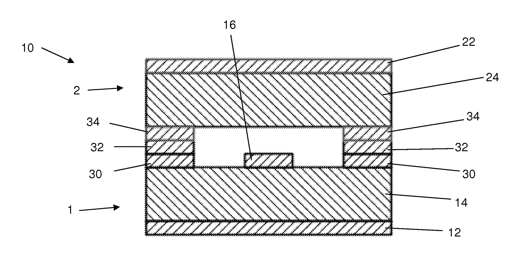
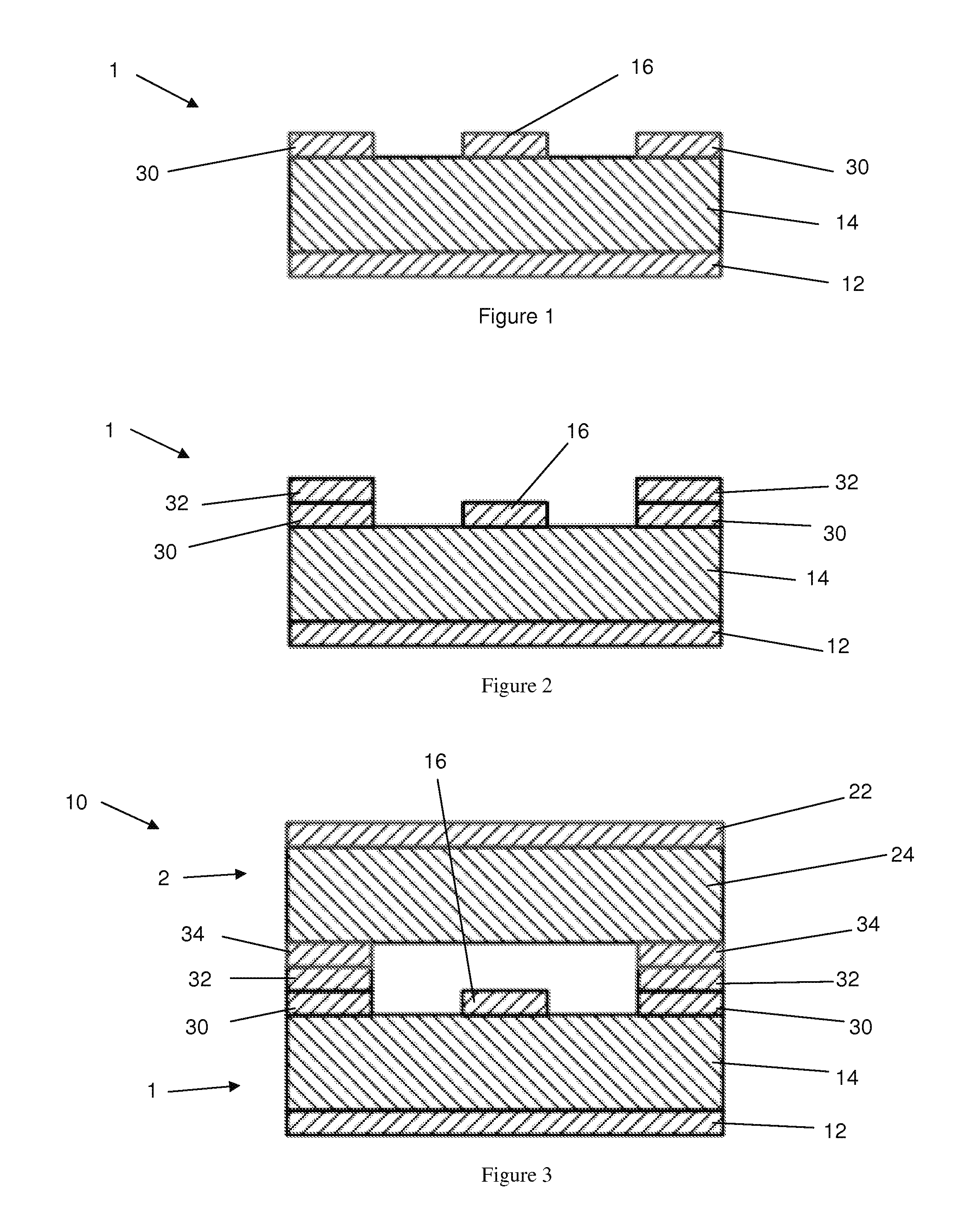
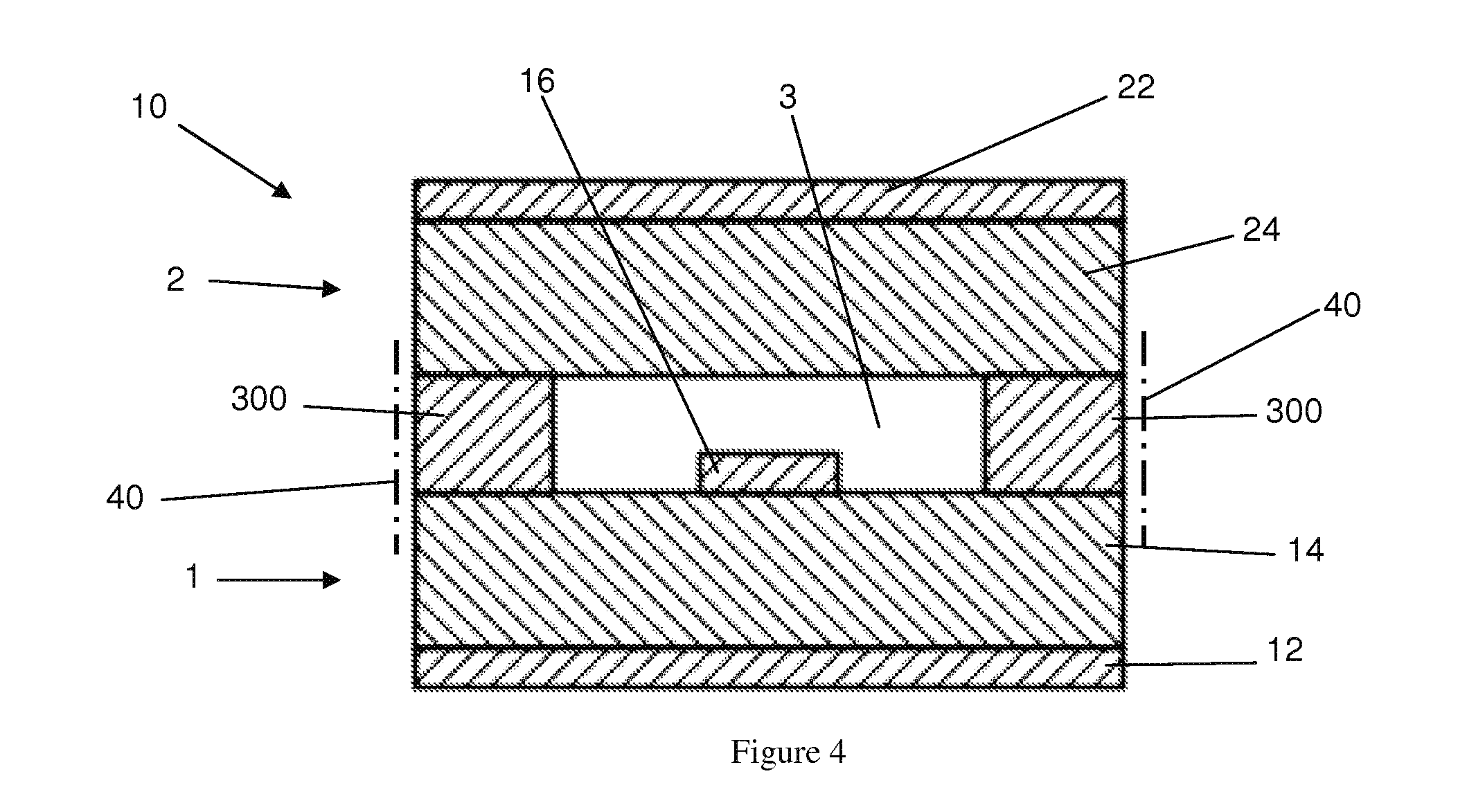
[0023]Reference will now be made in detail to the present exemplary embodiments of the invention, an example of which is illustrated in the accompanying drawings. Wherever possible, the same reference numbers will be used throughout the drawings to refer to the same or like parts. An exemplary embodiment of the stripline structure of the present invention is shown in FIG. 3, and is designated generally throughout by reference numeral 10.

[0024]Referring to FIG. 1, a cross-sectional view of a unit 1 with a pre-fired substrate 14 having printed artwork and a base metallization layer disposed thereon. Specifically, a transmission line structure 16 is disposed on one side of the pre-fired substrate and a ground metallization layer 12 is disposed on the opposite side of the pre-fired ceramic substrate 14 (forming a first unit 1). The bond layer 30 of metallic material is disposed around the periphery of the transmission line structure 16 in a 4-10 μm metal layer using a thick film process...


PUM

PropertyMeasurementUnit
thicknessaaaaaaaaaa
conductiveaaaaaaaaaa
mechanicalaaaaaaaaaa

Abstract

The present invention is directed to a stripline assembly that includes a first pre-fired ceramic substrate including a ground plane disposed on a first surface of the first pre-fired ceramic substrate. A second pre-fired ceramic substrate includes a ground plane disposed on a first surface thereof and a circuit disposed on a second surface of the second pre-fired ceramic substrate opposite the first surface. The circuit is disposed between the first pre-fired ceramic substrate and the second pre-fired ceramic substrate. A conductive bonding layer is disposed around the periphery of the circuit and between the first pre-fired ceramic substrate and the second pre-fired ceramic substrate.

Description

RELATED APPLICATION DATA[0001]The present application claims the benefit of U.S. provisional patent application No. 61 / 734,113, filed Dec. 6, 2012, and is hereby incorporated by reference in its entirety.BACKGROUND OF THE INVENTION[0002]1. Field of the Invention[0003]The present invention relates generally to RF circuits, and particularly to RF circuits using ceramic substrates.[0004]2. Technical Background[0005]A stripline circuit is used in RF and microwave circuit applications and is implemented by disposing a transmission line between two ground planes. A dielectric material is disposed between the transmission line conductor and each of the ground planes. Stripline structures are typically employed in the manufacture of directional couplers, baluns, power dividers and other such devices used in RF, microwave and millimeter wave circuits. Currently there are two industry accepted methods for manufacturing stripline transmission lines and RF / Microwave filters. The first method us...

Claims


Application Information

Patent Timeline
Patent Type & Authority Applications(United States)
IPC IPC(8): H01P3/08H01P11/00
CPCH01P11/00H01P3/085H01P3/088H01P11/003Y10T29/49016
Inventor O'NEIL, BENTONCOOK, ADAMSHAWLEY, BENJAMIN
Owner TTM TECH INC
Why Eureka
Try Eureka