Printed circuit board and method for manufacturing the same

a printed circuit board and printed circuit technology, applied in the direction of printed circuit manufacturing, printed circuit aspects, printed element electric connection formation, etc., can solve the problems of increasing the request for heat radiation, failing to suggest measures to increase the area of heat radiating via to improve the operation of the rf module, etc., to achieve the effect of increasing the area of heat radiating and improving heat radiation efficiency

Inactive Publication Date: 2014-06-26
SAMSUNG ELECTRO MECHANICS CO LTD
View PDF6 Cites 9 Cited by
  • Summary
  • Abstract
  • Description
  • Claims
  • Application Information

AI Technical Summary

Benefits of technology

[0010]The present invention has been made in an effort to provide a printed circuit board and a method for manufacturing the same, capable of increasing the area of a heat radiating via to thereby improve heat radiation efficiency.

Problems solved by technology

In the case of an RF module used in mobile communication, operations thereof become rapidly deteriorated as a semiconductor chip rises in temperature due to the heat generated therefrom.
Recently, as the semiconductor chip has an increase in use frequency, improvement in function, and a decrease in size, the heat generated from the semiconductor chip becomes a large problem, which leads to an increase in request for heat radiation.
However, in the case where the size of the heat radiating via is 100 μm or greater, if a plating process is performed by a copper filling plating method of the prior art, a large dimple may occur, and thus a multilayer substrate has difficulty in forming a stack via, and if the dimple is exposed to an outermost layer, this may cause a problem in mounting the semiconductor chip.
The foregoing printed circuit board and method for manufacturing the same disclose contents associated with a heat radiating via, but fail to suggest measures for increasing the area of the heat radiating via to thereby improve operations of the RF module.

Method used


Image

  • Printed circuit board and method for manufacturing the same
  • Printed circuit board and method for manufacturing the same
  • Printed circuit board and method for manufacturing the same

Examples


Embodiment Construction

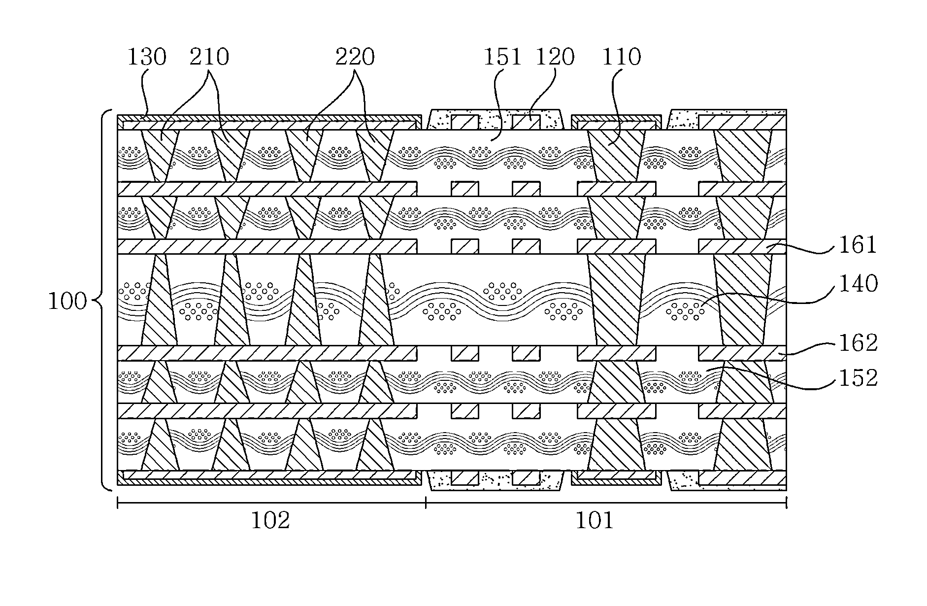
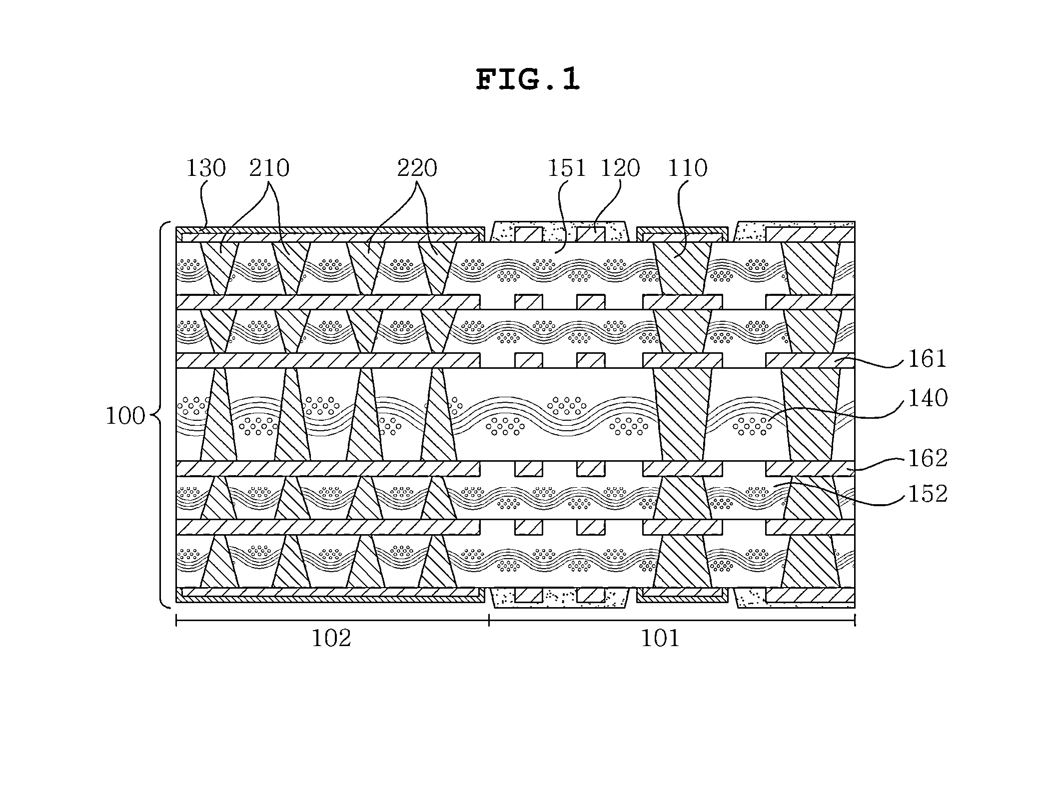
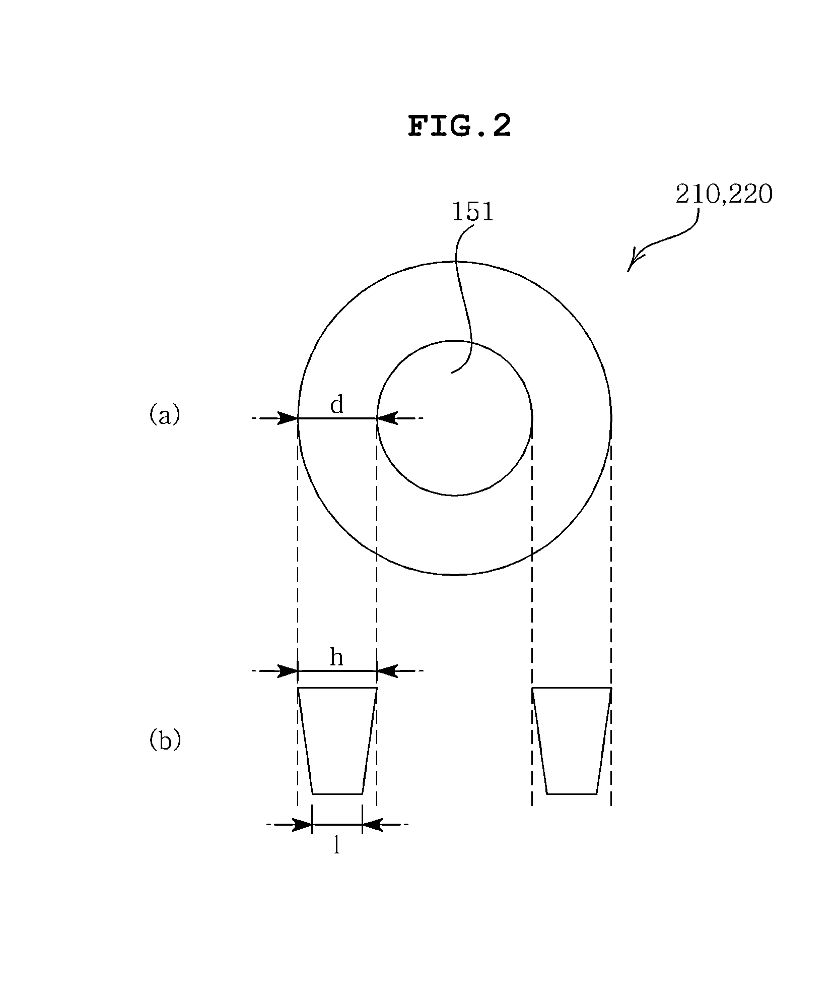
[0032]The objects, features and advantages of the present invention will be more clearly understood from the following detailed description of the preferred embodiments taken in conjunction with the accompanying drawings. Throughout the accompanying drawings, the same reference numerals are used to designate the same or similar components, and redundant descriptions thereof are omitted. Further, in the following description, the terms “first”, “second”, “one side”, “the other side”, and the like are used to differentiate a certain component from other components, but the configuration of such components should not be construed to be limited by the terms. Further, in the description of the present invention, when it is determined that the detailed description of the related art would obscure the gist of the present invention, the description thereof will be omitted.

[0033]Hereinafter, preferred embodiments of the present invention will be described in detail with reference to the atta...


PUM

PropertyMeasurementUnit
sizeaaaaaaaaaa
diameteraaaaaaaaaa
diameteraaaaaaaaaa

Abstract

Disclosed herein are a printed circuit board and a method for manfuacturing the same, the printed circuit board including: a base substrate having circuit patterns; and heat radiating vias having a donut shape, formed in the base substrate, so that the heat radiation efficiency may be improved by increasing the area of the heat radiating via.

Description

CROSS REFERENCE TO RELATED APPLICATION[0001]This application claims the benefit of Korean Patent Application No. 10-2012-0152982, filed Dec. 26, 2012, entitled “Printed Circuit Board and Method for Manufacturing Thereof”, and Korean Patent Application No. 10-2013-0048708, filed Apr. 30, 2013, entitled “Printed Circuit Board and Method for Manufacturing Thereof”, which are hereby incorporated by reference in their entireties into this application.BACKGROUND OF THE INVENTION[0002]1. Technical Field[0003]The present invention relates to a printed circuit board and a method for manufacturing the same.[0004]2. Description of the Related Art[0005]In the case of an RF module used in mobile communication, operations thereof become rapidly deteriorated as a semiconductor chip rises in temperature due to the heat generated therefrom. Therefore, in order to allow a substrate which has a semiconductor chip for an RF module mounted thereon to effectively remove the heat generated from the semico...

Claims


Application Information

Patent Timeline
Patent Type & Authority Applications(United States)
IPC IPC(8): H05K1/02H05K3/40
CPCH05K3/4038H05K1/0206H05K1/0207H05K1/0243H05K2201/096H05K2201/09854Y10T29/49165
Inventor OH, CHANG GUNPARK, HO SIKOH, HWA SUB
Owner SAMSUNG ELECTRO MECHANICS CO LTD
Why Eureka
Try Eureka