Electromagnetic interference filter and method of manufacturing the same

a technology of electromagnetic interference and filter, which is applied in the direction of transformer/inductance magnetic core, magnet, magnetic body, etc., can solve the problems of large amount of electromagnetic interference (emi) that may occur in the dc/dc converter, large amount of electromagnetic wave noise, electromagnetic wave noise, etc., and achieve the effect of increasing leakage inductance and

Inactive Publication Date: 2014-06-26
SAMSUNG ELECTRO MECHANICS CO LTD
View PDF5 Cites 4 Cited by
  • Summary
  • Abstract
  • Description
  • Claims
  • Application Information

AI Technical Summary

Benefits of technology

[0017]An aspect of the present invention provides an electromagnetic interference (EMI) filter capable of increasing leakage inductance and a method of manufacturing the same.

Problems solved by technology

In general, in the case of a flat panel display (FPD), a large amount of electromagnetic wave noise may occur due to a switching type power converter, an image board, a semiconductor device, or the like, included therein.
The SMPS performs a switching operation at a low frequency, which may cause electromagnetic wave noise.
In this case, a large amount of electromagnetic interference (EMI) may occur in the DC / DC converter due to a sudden change in current and voltage due to the switching operation, operating of a miniaturized image board and semiconductor device and high speed operations thereof, and the like.
In general, in the case of the common mode current, a large amount of common mode noise may be present therein within a relatively wide bandwidth, and in the case of the differential mode current, a large amount of differential mode noise may be present within a low frequency band.
In particular, in the case of the display device subject to power factor correction, a much larger amount of differential mode noise may appear in the low frequency band.
However, even in the case of using the existing EMI filter, many other filtering devices may be used, which may lead to increases in both size and cost in the implementation thereof.

Method used


Image

  • Electromagnetic interference filter and method of manufacturing the same
  • Electromagnetic interference filter and method of manufacturing the same
  • Electromagnetic interference filter and method of manufacturing the same

Examples


Embodiment Construction

[0047]Hereinafter, embodiments of the present invention will be described in detail with reference to the accompanying drawings. The invention may, however, be embodied in many different forms and should not be construed as being limited to the embodiments set forth herein.

[0048]Rather, these embodiments are provided so that this disclosure will be thorough and complete, and will fully convey the scope of the invention to those skilled in the art.

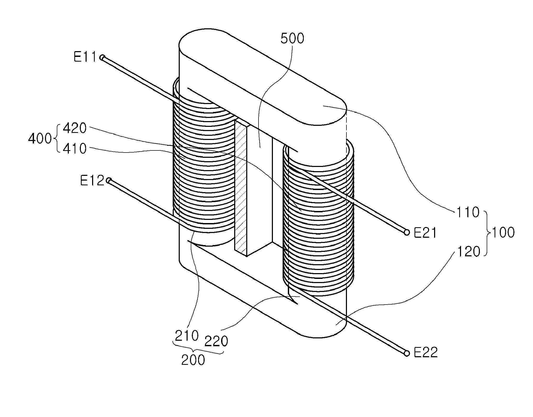
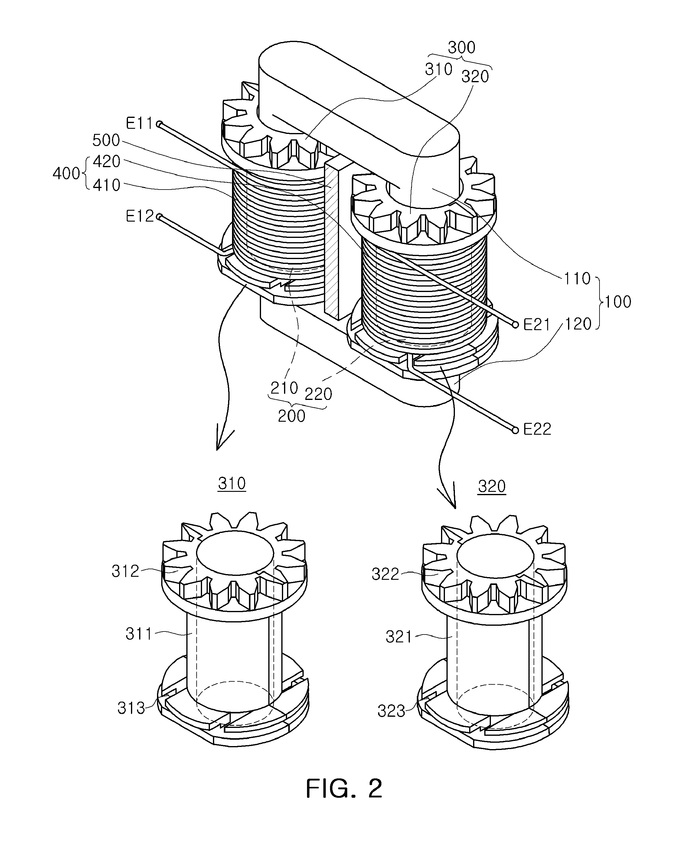
[0049]FIG. 1 is a structural diagram of an electromagnetic interference filter according to an embodiment of the present invention.

[0050]Referring to FIG. 1, the electromagnetic interference filter according to the embodiment of the present invention may include a base core 100, a leg core 200, a winding coil part 400, and a central core 500.

[0051]The base core 100 may include a first base core 110 and a second base core 120 facing the first base core 110.

[0052]The leg core 200 may include a first leg core 210 and a second leg core 220 form...


PUM

PropertyMeasurementUnit
frequencyaaaaaaaaaa
frequencyaaaaaaaaaa
frequencyaaaaaaaaaa

Abstract

There are provided an electromagnetic interference filter and a method of manufacturing the same. The electromagnetic interference filter includes a base core including a first base core and a second base core facing the first base core, a leg core including first and second leg cores disposed between the first base core and the second base core, the first and second leg cores facing each other, a winding coil part including first and second winding coils wound around the first and second leg cores, respectively, and connected to a power supply, the first and second winding coils respectively providing magnetizing inductance and leakage inductance, and a central core disposed between the first and second cores to provide an inductance leakage path between the first and second base cores.

Description

CROSS-REFERENCE TO RELATED APPLICATIONS[0001]This application claims priority from Korean Patent Application Nos. 10-2012-0151472 filed on Dec. 21, 2012 and 10-2013-0032734 filed on Mar. 27, 2013, in the Korean Intellectual Property Office, the disclosures of which are incorporated herein by reference in their entirety.BACKGROUND OF THE INVENTION[0002]1. Field of the Invention[0003]The present invention relates to an electromagnetic interference (EMI) filter capable of being applied to a flat panel display (FPD) and a method of manufacturing the same.[0004]2. Description of the Related Art[0005]In general, in the case of a flat panel display (FPD), a large amount of electromagnetic wave noise may occur due to a switching type power converter, an image board, a semiconductor device, or the like, included therein. In order to suppress the electromagnetic wave noise, an electromagnetic interference (EMI) filter may generally be used.[0006]The electromagnetic interference filter may be ...

Claims


Application Information

Patent Timeline
Patent Type & Authority Applications(United States)
IPC IPC(8): H01F3/12H01F41/02H03H3/00
CPCH01F3/12H01F27/325H01F2003/106H03H7/427H03H2001/0028H03H2001/0035Y10T29/49071
Inventor WON, JAE SUNHAN, SEUNG HOEOM, JAE GENCHIN, HWA HUNKIM, TAE HOONYU, SEUNG WAN
Owner SAMSUNG ELECTRO MECHANICS CO LTD
Why Eureka
Try Eureka