Receiver circuit with de-emphasis function

a receiver circuit and function technology, applied in the field of semiconductor design technology, can solve the problems of data interference, inter-symbol interference (isi), incorrect delivery, etc., and achieve the effect of efficient compensation of distorted input signals

Active Publication Date: 2014-06-26
SK HYNIX INC
View PDF9 Cites 62 Cited by
  • Summary
  • Abstract
  • Description
  • Claims
  • Application Information

AI Technical Summary

Benefits of technology

[0015]The receiver circuit in accordance with an embodiment of the preset invention may perform in a high-frequency region. The receiver circuit may efficiently compensate the distorted input signal by a de-emphasis equalization method.

Problems solved by technology

Further, interference between the data, i.e., inter-symbol interference (ISI) arises.
That is, since the time at which the digital signal is arrived may differ depending on frequency components due to the channel loss, successive data may overlap, which may result in incorrect delivery in a case of high-speed communication or a long-channel communication.

Method used


Image

  • Receiver circuit with de-emphasis function
  • Receiver circuit with de-emphasis function
  • Receiver circuit with de-emphasis function

Examples


Embodiment Construction

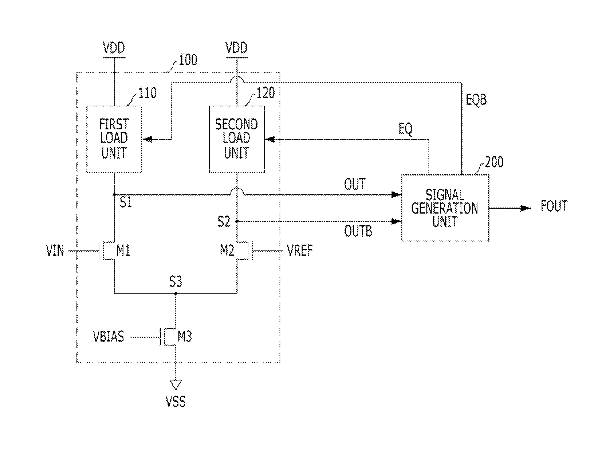
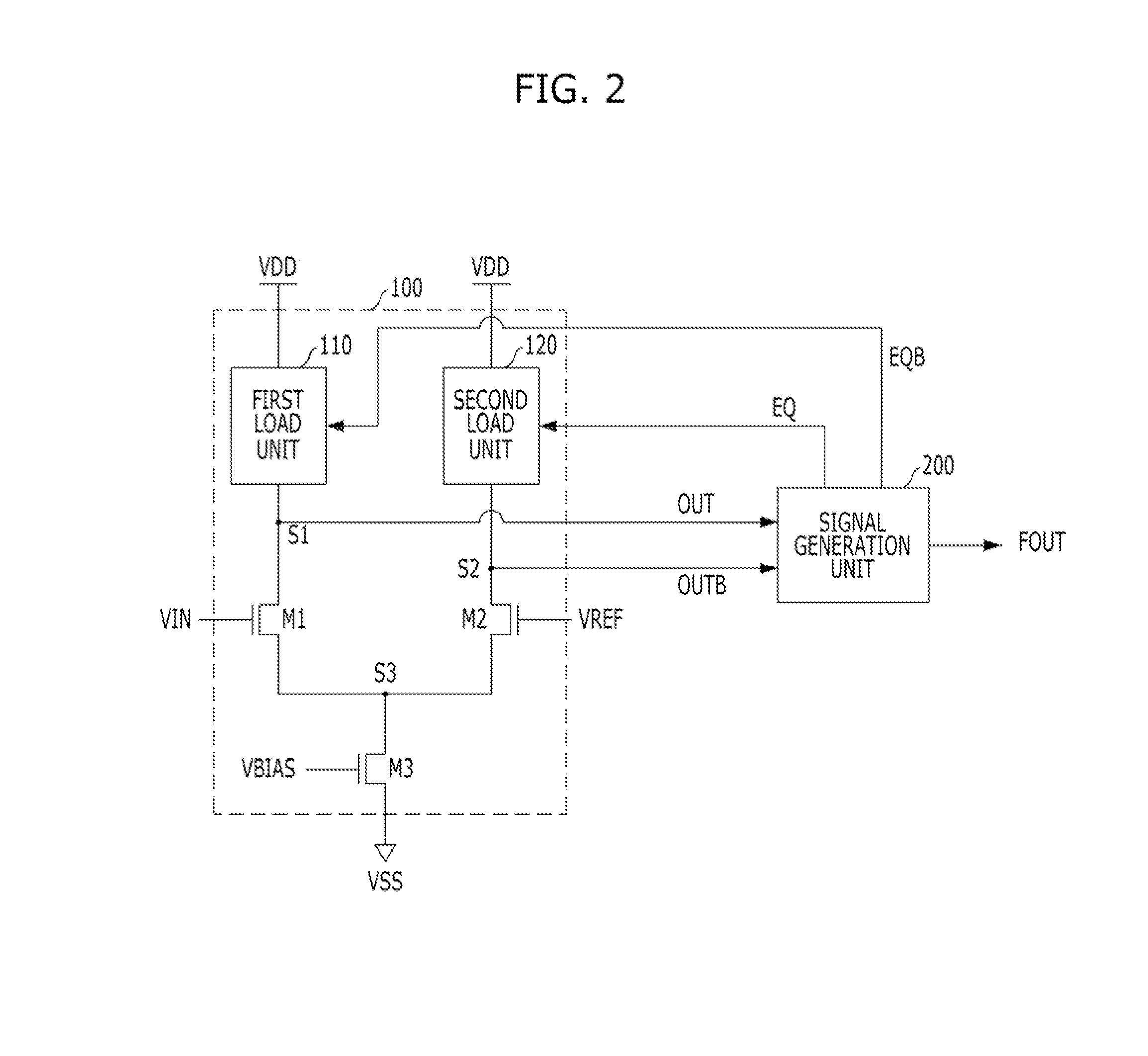
[0020]Hereinafter, embodiments of the present invention will be described in detail with reference to the accompanying drawings. However, the present invention is not limited to embodiments described below, but may be configured in various other forms. Therefore, the present embodiments are provided to complete the disclosure of the present invention and fully inform those skilled in the art of the scope of the present invention. Throughout the disclosure, reference numerals correspond directly to the like numbered parts in the various figures and embodiments of the present invention. It is also noted that in this specification, connected / coupled refers to one component not only directly coupling another component but also indirectly coupling another component through an intermediate component. In addition, a singular form may include a plural form as long as it is not specifically mentioned in a sentence.

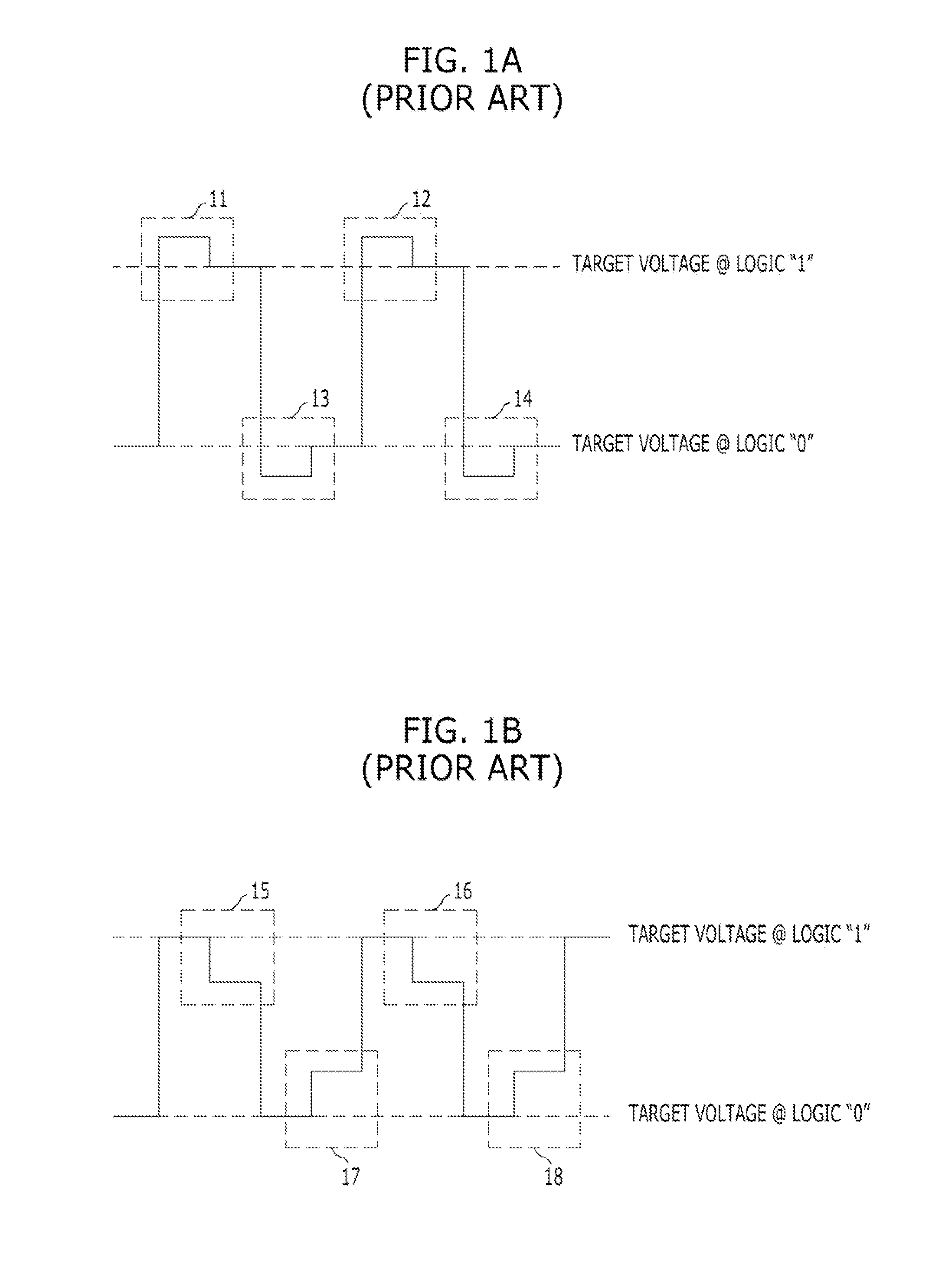
[0021]For reference, a logic signal of a circuit and a value of a binary data ...


PUM


Abstract

A receiver circuit includes a first differential amplification unit including a variable load section, and configured to receive first and second input signals, and to generate first and second output signals, which are amplified based on an impedance value of the variable load section and a voltage difference between the first and second input signals, a second differential amplification unit configured to receive the first and second output signals and to generate a third output signal based on a voltage difference between the first and second output signals, and a signal generating unit configured to generate an equalization signal for controlling the variable load section based on the third output signal.

Description

CROSS-REFERENCE TO RELATED APPLICATIONS[0001]The present application claims priority of Korean Patent Application No. 10-2012-0152860 filed on Dec. 24, 2012, which is incorporated herein by reference in its entirety.BACKGROUND[0002]1. Field[0003]Exemplary embodiments of the present invention relate to semiconductor design technology, and more particularly to a receiver circuit with a de-emphasis function.[0004]2. Description of the Related Art[0005]In integrated circuits, such as semiconductor memory devices, an operating voltage becomes lower, and a speed of transmitted signals gradually increases. When a transmitter transmits a digital signal through a channel having a loss, a receiver receives the transmitted signal in a state that is distorted depending on frequency components of the channel.[0006]In general, since a channel has more losses in a high-frequency region, high-frequency components of a digital signal transmitted through the channel are attenuated more than low-frequ...

Claims


Application Information

Patent Timeline
Patent Type & Authority Applications(United States)
IPC IPC(8): H04L25/03
CPCH04L25/0272G11C7/06G11C7/10
Inventor HWANG, TAE-JIN
Owner SK HYNIX INC
Why Eureka
Try Eureka