Pixel circuit and display device

a pixel circuit and display device technology, applied in the field of pixel circuits, can solve the problems of difficult to obtain uniform properties of the tfts forming the pixel circuits for the entire display panel, variable luminance, deterioration of display quality, etc., and achieve the effect of enhancing the degree of freedom in arranging transistors and the like within a pixel, affecting the electrical mobility of the transistor, and easy equalization

Active Publication Date: 2009-01-13
SANYO ELECTRIC CO LTD
View PDF5 Cites 36 Cited by
  • Summary
  • Abstract
  • Description
  • Claims
  • Application Information

AI Technical Summary

Benefits of technology

[0012]The present invention provides a pixel circuit to effectively compensate for difference in threshold voltage of a driving transistor with a simple change.

Problems solved by technology

In such a pixel circuit, however, variation in threshold voltage among the driving TFTs of the pixel circuits arranged in a matrix results in variation in luminance and deterioration in display quality.
It is difficult to obtain uniform properties of the TFTs forming the pixel circuits for the entire display panel, and therefore to prevent variation in ON / OFF threshold.

Method used


Image

  • Pixel circuit and display device
  • Pixel circuit and display device
  • Pixel circuit and display device

Examples


Embodiment Construction

[0046]An embodiment of the present invention will now be described with reference to the accompanying drawings.

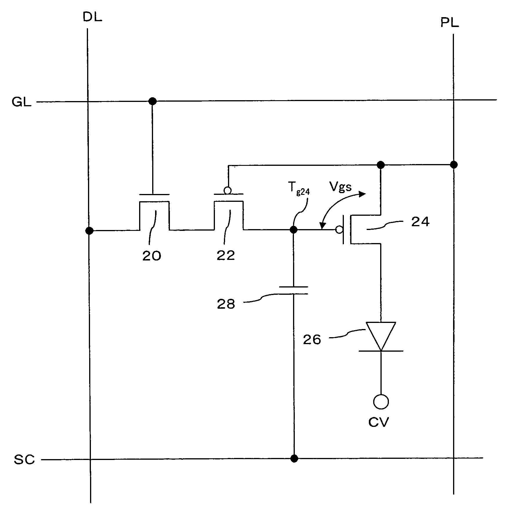
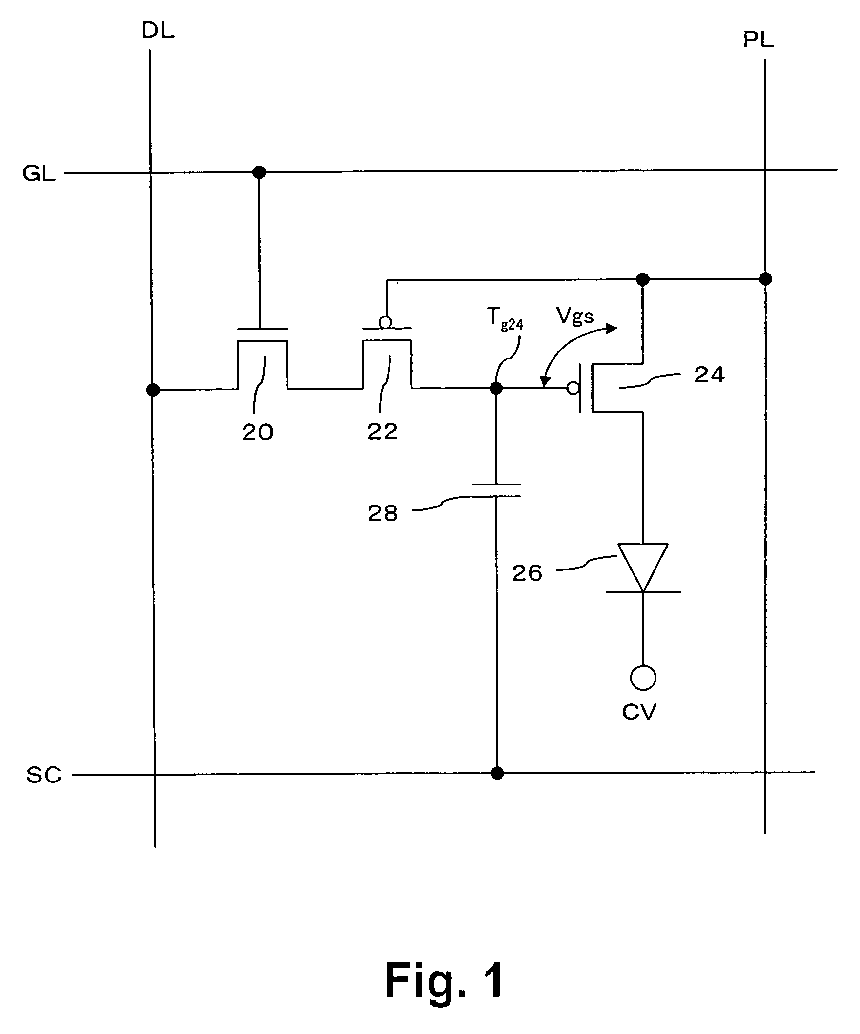
[0047]FIG. 1 shows a configuration of a pixel circuit per pixel according to an embodiment. A data line DL extending in a vertical scanning direction is connected to a first conductive region (drain) of an n-channel selection TFT 20. The selection TFT 20 has a gate (control end) connected to a gate line GL extending in a horizontal scanning direction, and a second conductive region (source) connected to a first conductive region (source) of a p-channel correction TFT 22. The selection TFT 20 may have a p-channel, and for the p-channel TFT, the polarity (H level or L level) of a selection signal (gate signal) provided to the gate line GL will be inverted for driving the transistor.

[0048]A control end (gate) of the correction TFT 22 is connected to a power source line PL (voltage Pvdd), and a second conductive region (drain) is connected to a control end (gate) of a p-channel...


PUM


Abstract

When a selection TFT and a correction TFT are turned on, a data voltage of a data line is stored in a storage capacitor as a gate voltage of a driving TFT. After turning off the selection TFT, a voltage of a capacitor line SC falls, thereby turning on the driving TFT to supply a driving current to an organic EL element. The correction TFT is in the ON state before the capacitor line SC falls, and is turned off in the course of the fall of the line. Consequently, the capacitance of the correction TFT changes during the fall of the gate voltage, and the gradient of the gate voltage fall of the driving TFT is changed, thereby setting the gate voltage after the capacitor line SC falls in accordance with variation in threshold of the driving TFT. Particularly by disposing the driving TFT and the correction TFT adjacent to each other, the two TFTs are provided with the same properties to achieve effective correction.

Description

TECHNICAL FIELD[0001]The present invention relates to a pixel circuit including an emissive element, such as an organic EL element, and a display device having such pixel circuits arranged in a matrix.BACKGROND ART[0002]Organic EL panels using organic EL elements as emissive elements have been known and actively developed. In such an organic EL panel, organic EL elements are arranged in a matrix, and light emission from these organic EL elements is individually controlled to display an image. Particularly, an organic EL panel of an active matrix type includes a TFT for display control for each pixel, and light emission is controlled for each pixel by controlling operation of the TFT, thereby achieving a very high resolution display.[0003]FIG. 13 shows an example of a pixel circuit in an organic EL panel of the active matrix type. A data line receiving a data voltage indicating luminance of a pixel is connected to a gate of a driving TFT 12 through an n-channel selection TFT 10 whose...

Claims


Application Information

Patent Timeline
Patent Type & Authority Patents(United States)
IPC IPC(8): G09G3/30G09G3/10H01L51/50G09F9/30G09G3/20G09G3/32H01L27/32H05B33/14
CPCG09G3/3233G09G2300/0417G09G2300/0426G09G2300/0819H01L27/3244G09G2300/0876G09G2320/0233G09G2320/043G09G2300/0842H10K59/12G09G3/30G09G3/20H05B33/12
Inventor KOGA, MASAYUKIMARUMO, KOJI
Owner SANYO ELECTRIC CO LTD
Why Eureka
Try Eureka