Computation Memory Operations in a Logic Layer of a Stacked Memory

a logic layer and memory technology, applied in the field of computer systems, can solve the problems of limiting the opportunity to optimize memory accesses and data transfers, consuming power for the transmission of memory addresses and associated commands, and introducing performance overheads, so as to achieve the effect of increasing performance and/or power efficiency

Active Publication Date: 2014-06-26
ADVANCED MICRO DEVICES INC
View PDF4 Cites 13 Cited by
  • Summary
  • Abstract
  • Description
  • Claims
  • Application Information

AI Technical Summary

Benefits of technology

[0010]Embodiments use die-stacked memories that contain a logic layer in addition to one or more layers of DRAM (or other memory technology). This logic layer can be a discrete logic die or logic on a silicon interposer associated with a stack of memory dies. Embodiments place additional circuitry/functionality on the

Problems solved by technology

The transmission of the memory addresses and associated commands consumes power and may introduce performance overheads in cases where the address/command bandwidth becomes a bottleneck.
Furthermore, issuing addresses and control commands on a per-data-item basis may limit opportunities to optimize memory accesses and data transfers.
Past proposals to implement additional logic directly in the memory are expensive and have not proven to be practical because the placement of logic in a memory chip incurs significant cos

Method used


Image

  • Computation Memory Operations in a Logic Layer of a Stacked Memory
  • Computation Memory Operations in a Logic Layer of a Stacked Memory
  • Computation Memory Operations in a Logic Layer of a Stacked Memory

Examples


Embodiment Construction

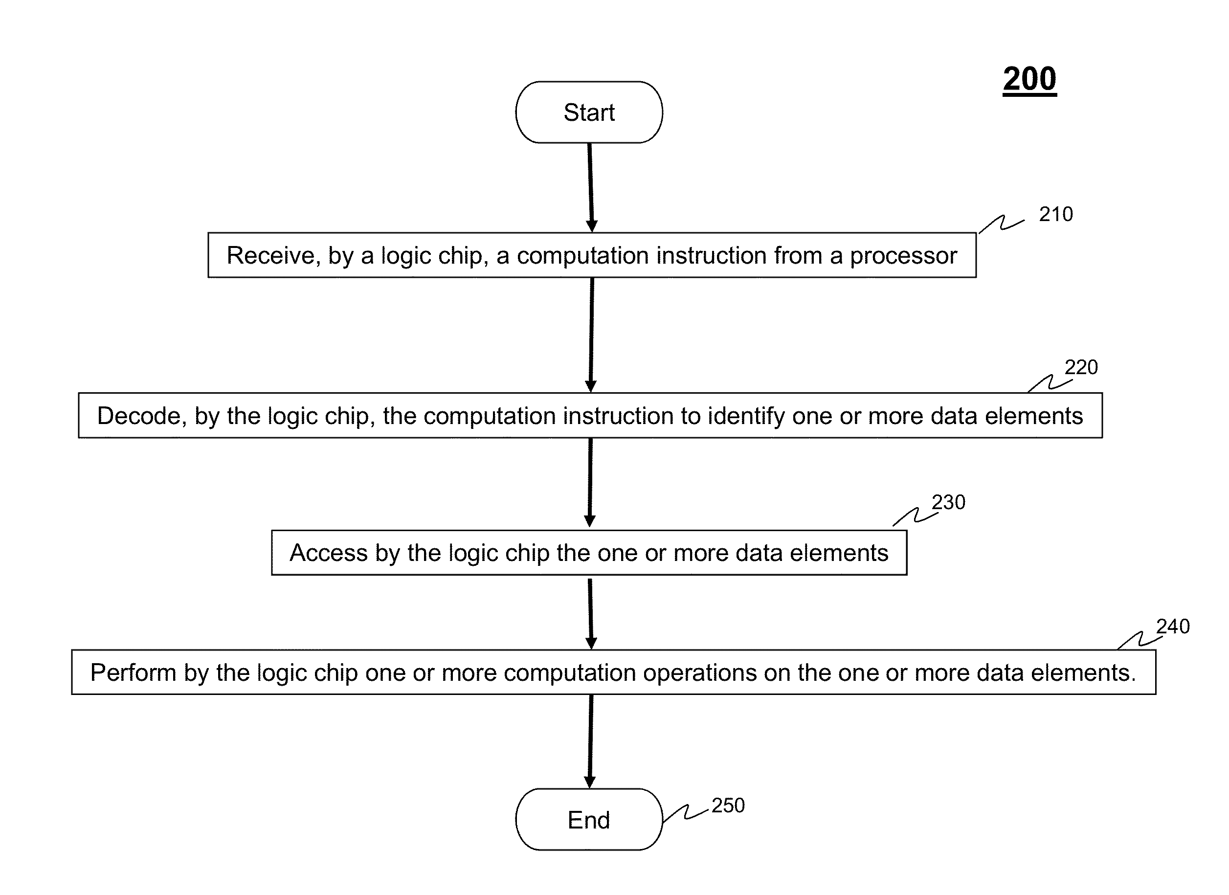
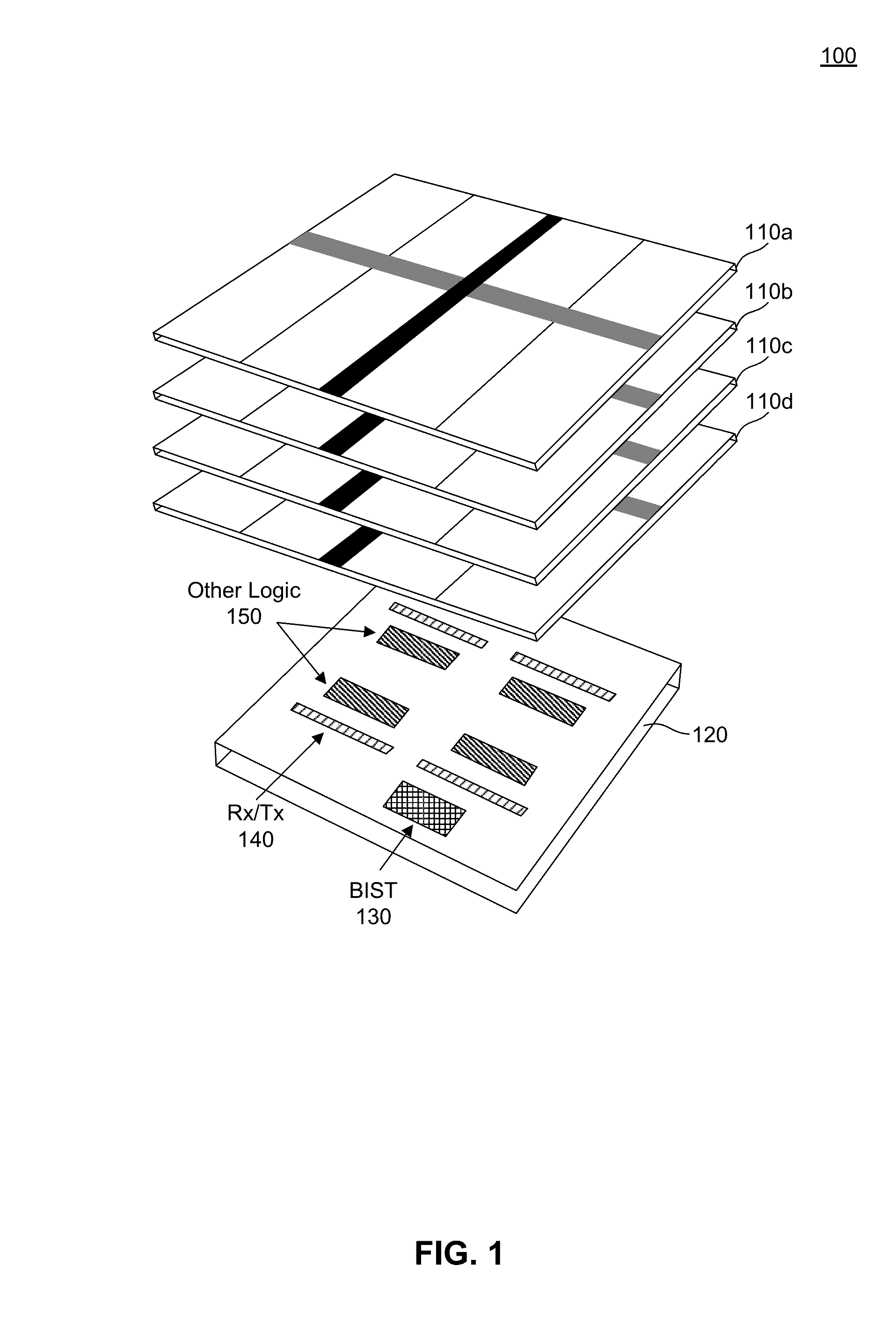
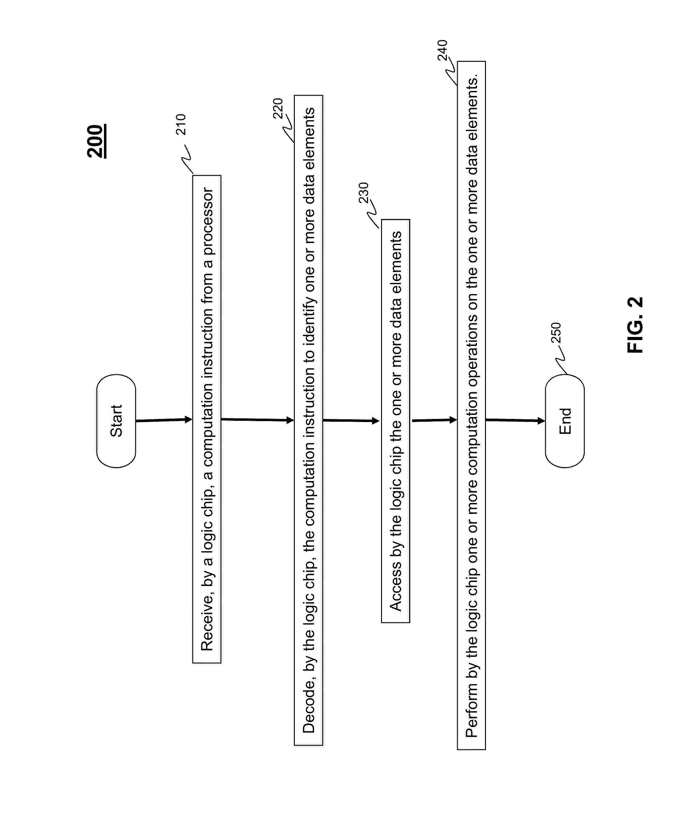
[0008]Therefore, what is needed are memory systems using multiple silicon chips within a single package, for example a memory chip three-dimensionally integrated with a logic / interface chip. The additional logic chip provides opportunities to integrate additional functionality not normally provided by memory systems. The functionality of this logic chip could be implemented on a silicon interposer on which the memory chips as well as other processing chips are stacked.

[0009]Embodiments use the logic functions to implement additional functionality to perform data computations associated with data in the associated memory chips. For instance, a reduction operation that computes the maximum value in an array can be performed in the logic associated with a memory stack to read the memory elements associated with an array, compute the maximum value, and return only this maximum value to the host processor.

[0010]Embodiments use die-stacked memories that contain a logic layer in addition t...


PUM


Abstract

Some die-stacked memories will contain a logic layer in addition to one or more layers of DRAM (or other memory technology). This logic layer may be a discrete logic die or logic on a silicon interposer associated with a stack of memory dies. Additional circuitry/functionality is placed on the logic layer to implement functionality to perform various computation operations. This functionality would be desired where performing the operations locally near the memory devices would allow increased performance and/or power efficiency by avoiding transmission of data across the interface to the host processor.

Description

BACKGROUND[0001]1. Field[0002]The disclosed embodiments relate generally to computer systems, and in particular to computation memory operations in memory management.[0003]2. Background Art[0004]Computer systems of various types are ubiquitous in modern society. Common to these computer systems is the storage of data in memory, from which processors perform read, write and other access instructions. Considerable portions of resources in computer systems are employed with the execution of these instructions.[0005]Computer systems typically use processors, where the term “processor” generically refers to anything that accesses memory in a computing system. Processors typically load and store data to / from memory by issuing addresses and control commands on a per-data-item basis. Here a data item may be a byte, a word, a cache line, or the like, as the particular situation requires. These data accesses require a separate address and one or more commands to be transmitted from the proces...

Claims


Application Information

Patent Timeline
IPC IPC(8): G06F9/30
CPCG06F15/7821Y02D10/00
Inventor O'CONNOR, JAMES M.JAYASENA, NUWAN S.LOH, GABRIEL H.IGNATOWSKI, MICHAELSCHULTE, MICHAEL J.
Owner ADVANCED MICRO DEVICES INC
Why Eureka
Try Eureka