
Multilayer ceramic capacitor and method of manufacturing the same

a multi-layer ceramic and capacitor technology, applied in the field can solve problems such as the reliability decline of multi-layer ceramic capacitors

Active Publication Date: 2014-07-24
SAMSUNG ELECTRO MECHANICS CO LTD
View PDF0 Cites 45 Cited by
  • Summary
  • Abstract
  • Description
  • Claims
  • Application Information

AI Technical Summary

Benefits of technology

The present invention is about improving the performance of a multilayer ceramic capacitor. The invention addresses the issue of interface separation between the conductive resin layer and electrodes, as well as the conductive resin layer and plating layer in the external electrode. The described method of manufacturing the capacitor improves these interface separations, ultimately resulting in a more reliable and efficient multilayer ceramic capacitor.

Problems solved by technology

In particular, this interface separation is frequently generated during a process of mounting the multilayer ceramic capacitor on a substrate, thereby decreasing reliability of the multilayer ceramic capacitor.

Method used


Image

  • Multilayer ceramic capacitor and method of manufacturing the same
  • Multilayer ceramic capacitor and method of manufacturing the same
  • Multilayer ceramic capacitor and method of manufacturing the same

Examples


experimental example

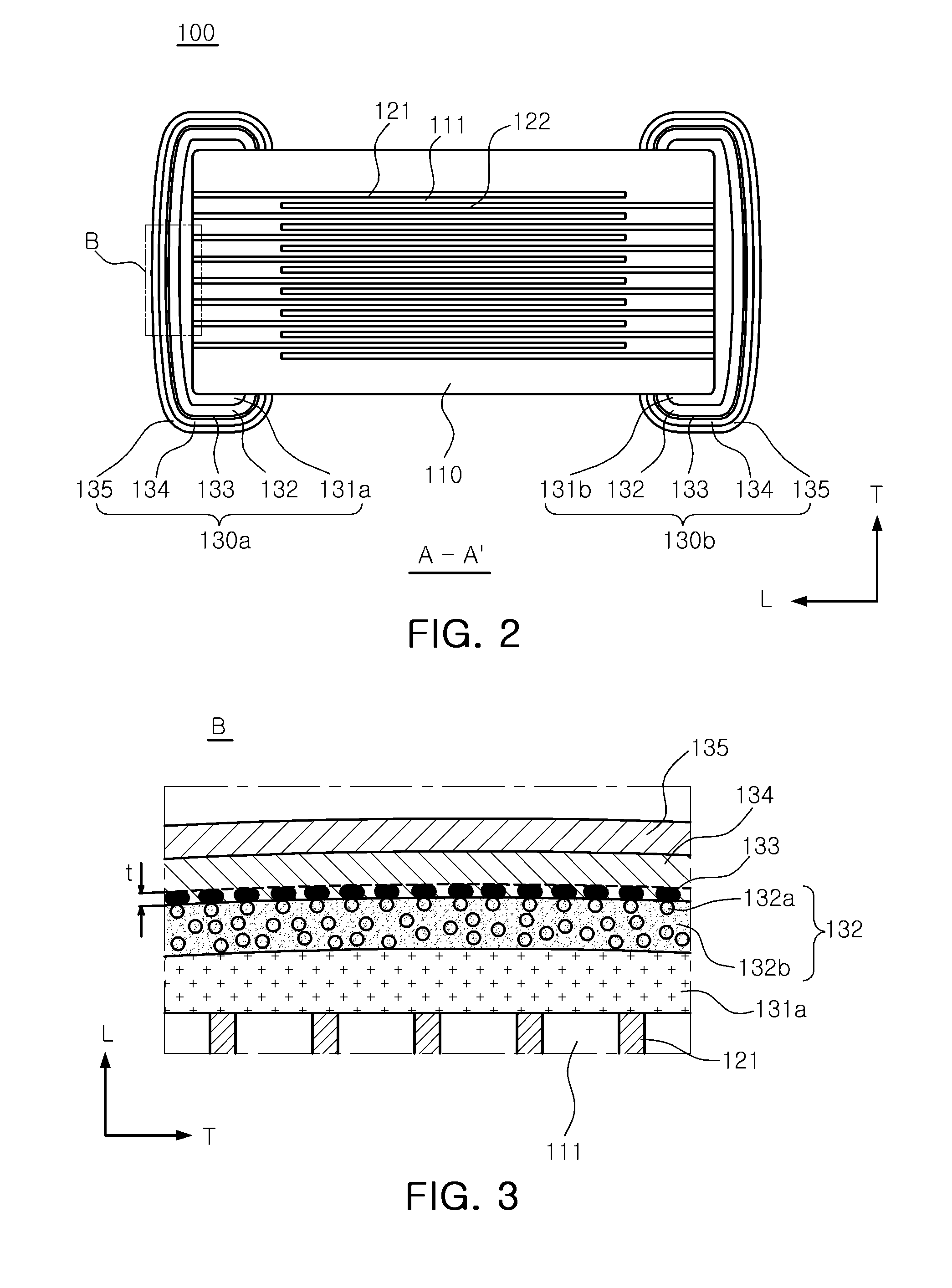
[0067]The following Table 1 shows results obtained by evaluating interface adhesive force between an electrode layer and a conductive resin layer (referred to as ‘adhesion at inner interface’ in Table 1) and interface adhesive force between the conductive resin layer and a nickel plating layer (referred to as ‘adhesion at outer interface’ in Table 1) according to thicknesses of copper-nickel alloy layers.

[0068]Evaluation of the interface adhesive force was performed by a soldering bath test. When the manufactured multilayer ceramic capacitor was immersed in a soldering bath at 300° C. for 10 minutes to apply instant thermal impact thereto, whether or not interface separation occurred was measured. In the following Table 1, the case in which interface separation occurred was represented by “NG” and the case in which interface separation did not occur was represented by “OK”

TABLE 1Thickness ofcopper-nickel alloy Adhesion atAdhesion atSamplelayer (nm)inner interfaceouter interface1*0.5...


PUM

PropertyMeasurementUnit
Thicknessaaaaaaaaaa
Nanoscale particle sizeaaaaaaaaaa
Electrical conductoraaaaaaaaaa

Abstract

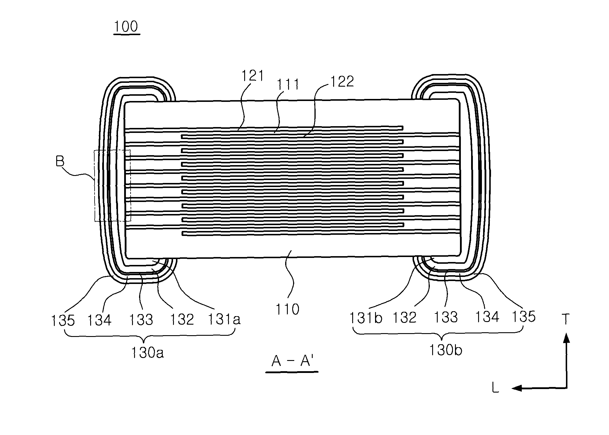
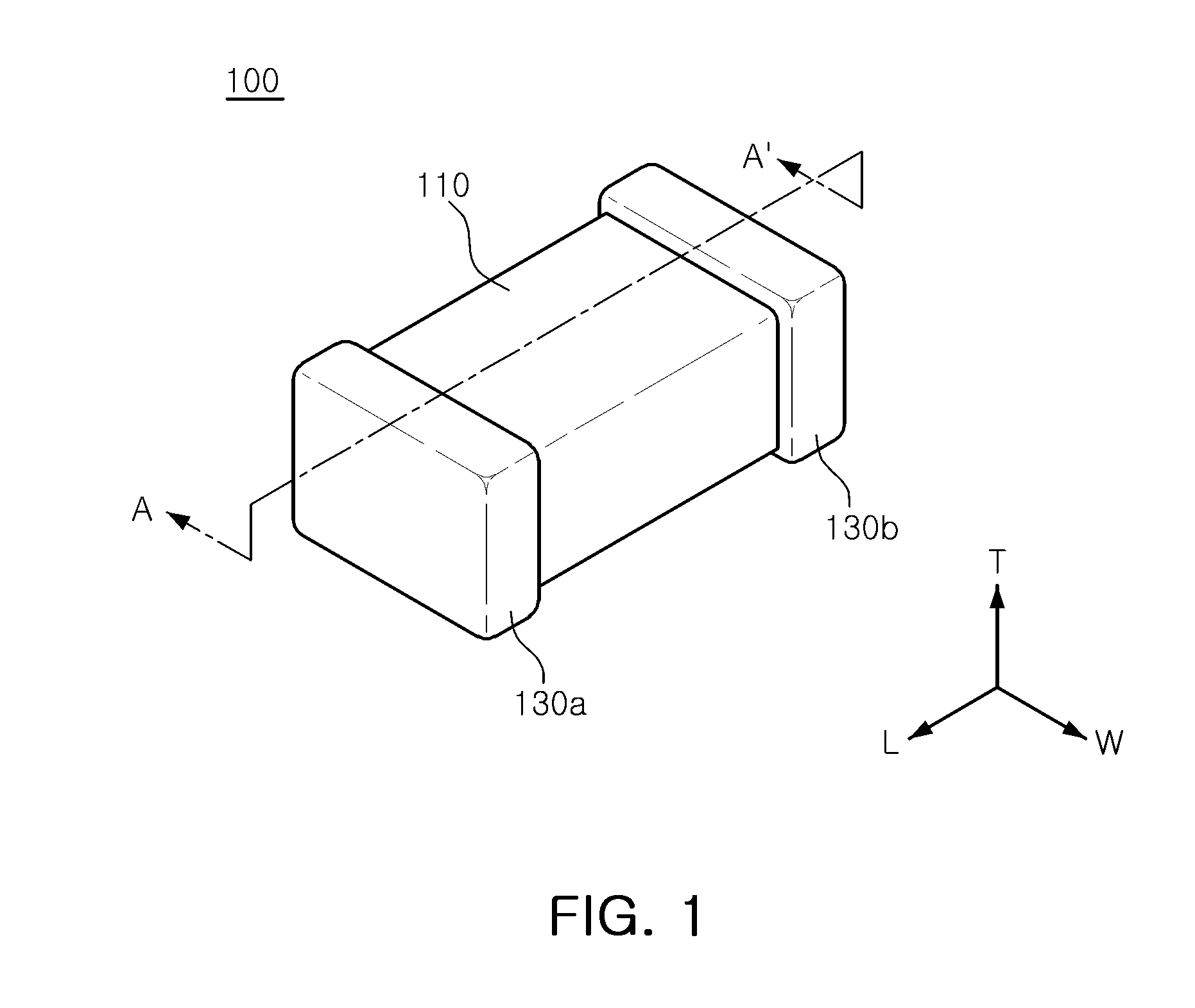
There is provided a multilayer ceramic capacitor including a ceramic body including dielectric layers, first and second internal electrodes formed within the ceramic body and disposed to face each other, having the dielectric layer interposed therebetween, first and second electrode layers disposed on outer surfaces of the ceramic body and electrically connected to the first and second internal electrodes, respectively, a conductive resin layer disposed on the first and second electrode layers and containing copper powder, a nickel plating layer disposed on an outer portion of the conductive resin layer, and a copper-nickel alloy layer disposed between the conductive resin layer and the nickel plating layer and having a thickness of 1 to 10 nm.

Description

CROSS-REFERENCE TO RELATED APPLICATIONS[0001]This application claims the priority of Korean Patent Application No. 10-2013-0008259 filed on Jan. 24, 2013, in the Korean Intellectual Property Office, the disclosure of which is incorporated herein by reference.BACKGROUND OF THE INVENTION[0002]1. Field of the Invention[0003]The present invention relates to a multilayer ceramic capacitor in which interface separation phenomena between a conductive resin layer included in an external electrode and an electrode layer, and between the conductive resin layer and a plating layer, are decreased, and a method of manufacturing the same.[0004]2. Description of the Related Art[0005]In general, among ceramic electronic components, a multilayer ceramic capacitor includes a plurality of stacked dielectric layers, internal electrodes disposed to face each other, having the dielectric layer interposed therebetween, and external electrodes electrically connected to respective internal electrodes.[0006]...

Claims


Application Information

Patent Timeline
IPC IPC(8): H01G4/008
CPCH01G4/008H01G4/12H01G4/232H01G4/2325H01G4/30Y10T29/43
Inventor CHUN, BYOUNG JINJEON, BYUNG JUNHONG, KYUNG PYOHAN, JAE HWAN
Owner SAMSUNG ELECTRO MECHANICS CO LTD
Learn More