Apparatus and method of detecting a defect of a semiconductor device

a semiconductor device and apparatus technology, applied in the field of semiconductor devices, can solve problems such as pattern deformation and increase cracking

Inactive Publication Date: 2014-07-31
SAMSUNG ELECTRONICS CO LTD
View PDF4 Cites 32 Cited by
  • Summary
  • Abstract
  • Description
  • Claims
  • Application Information

AI Technical Summary

Problems solved by technology

However, as the thicknesses of semiconductor packages, wafers and chips become smaller, there is an increase in cracking, pattern

Method used


Image

  • Apparatus and method of detecting a defect of a semiconductor device
  • Apparatus and method of detecting a defect of a semiconductor device
  • Apparatus and method of detecting a defect of a semiconductor device

Examples


Embodiment Construction

[0041]Hereinafter, exemplary embodiments of the inventive concept will be described in detail with reference to the accompanying drawings. The inventive concept may, however, be embodied in many different forms and should not be construed as limited to the embodiments set forth herein.

[0042]When an element is referred to as being “connected” to another element, it can be directly connected to the other element or intervening elements may be present. When an element is referred to as being “on” another element, the element can be directly on another element or intervening elements may be present. In the drawings, the structure or size of each element may be exaggerated for clarity. Like numbers may refer to like elements throughout the specification and drawings.

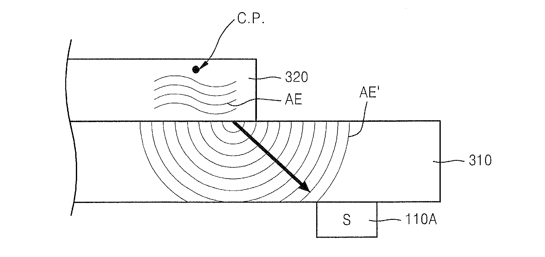
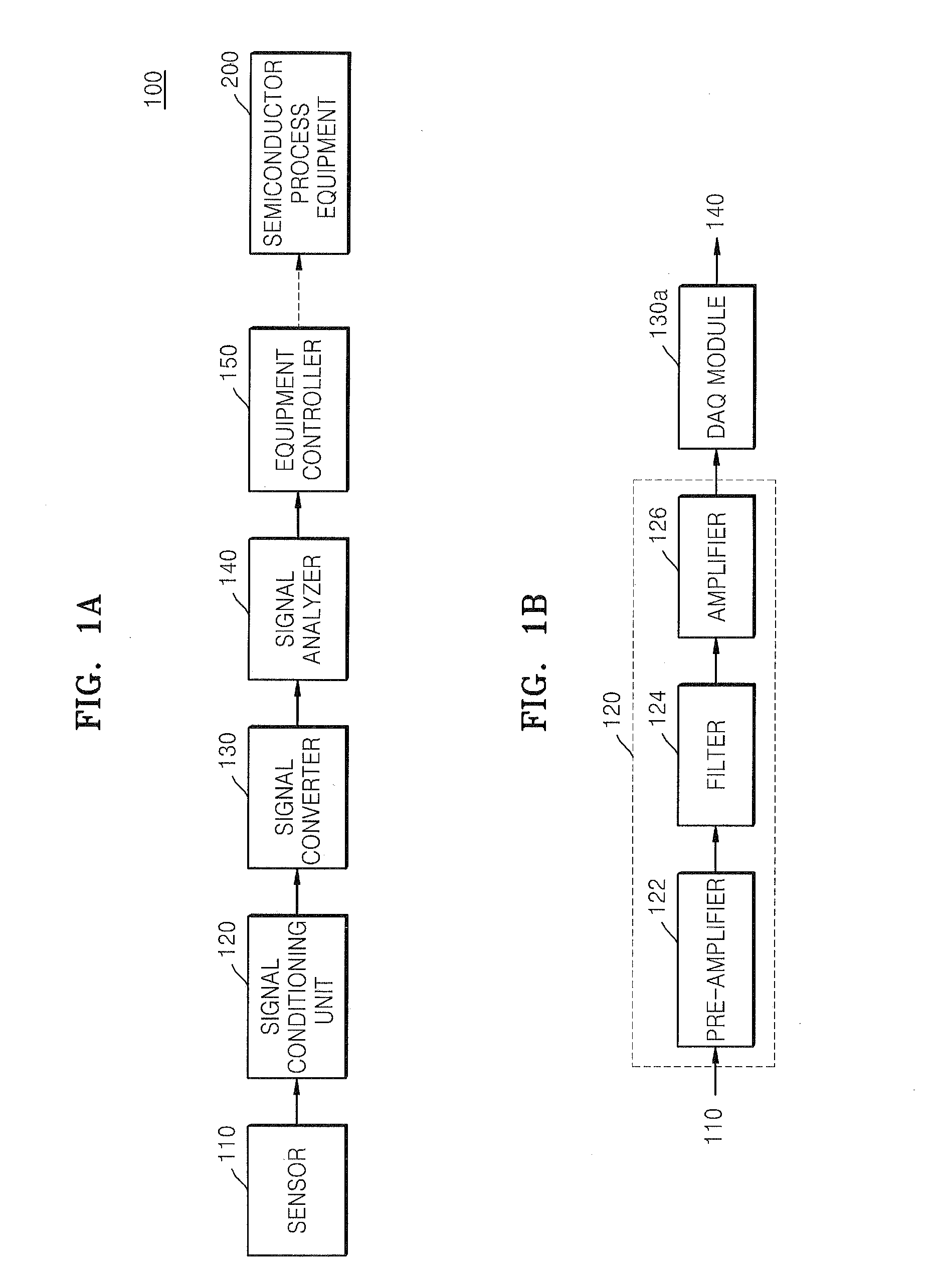
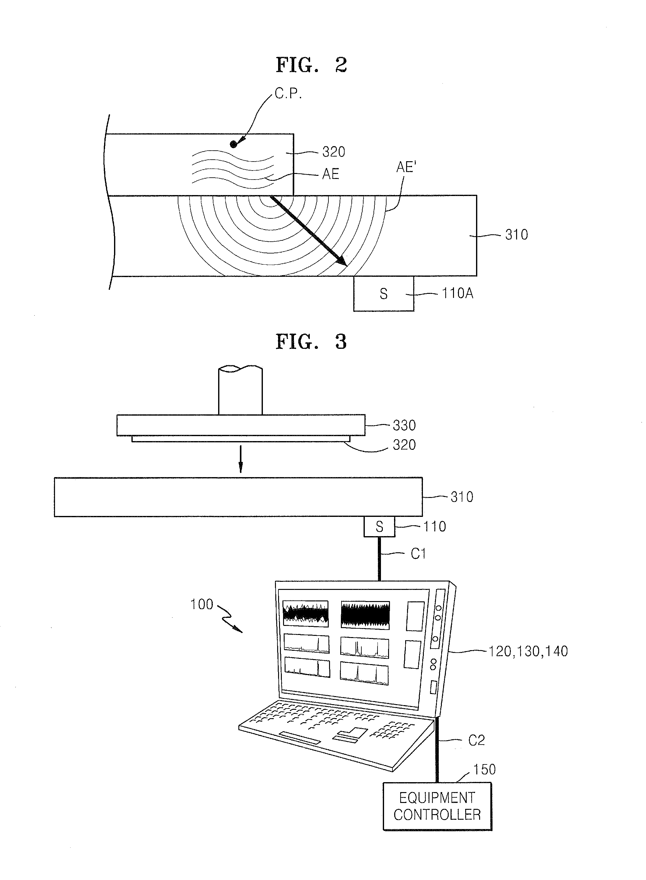
[0043]FIG. 1A is a block diagram of a semiconductor device defect detecting apparatus 100 according to an exemplary embodiment of the inventive concept.

[0044]Referring to FIG. 1A, the semiconductor device defect detecting app...


PUM


Abstract

A semiconductor device defect detecting apparatus including: a sensor disposed on semiconductor process equipment, the sensor configured to detect a signal emitted from a semiconductor device in contact with the semiconductor process equipment; and a signal analyzer configured to determine whether the semiconductor device is defective based on the detected signal in a predetermined frequency range.

Description

BACKGROUND[0001]1. Technical Field[0002]The inventive concept relates to semiconductor devices and methods of manufacturing the same, and more particularly, to an apparatus and method of detecting a defect of a semiconductor device.[0003]2. Discussion of the Related Art[0004]To meet the demand for semiconductor devices with high-speed operations and large-capacity data storage, semiconductor device manufacturing technology has been developed. In addition, semiconductor device manufacturing technology has been developed to meet the demand for thin semiconductor devices. However, as the thicknesses of semiconductor packages, wafers and chips become smaller, there is an increase in cracking, pattern deformation, or the like occurring in a semiconductor package, a wafer or a chip in a semiconductor device manufacturing process.SUMMARY[0005]Exemplary embodiments of the inventive concept provide a semiconductor device defect detecting apparatus and a semiconductor device defect detecting ...

Claims


Application Information

Patent Timeline
IPC IPC(8): G01N29/14
CPCG01N29/14G01N2291/0289H01L21/00G01N29/4454H01L21/67288G01N29/04G01R31/26G01R31/265
Inventor KIM, GEUN-WOOKIM, HYUNYOO, YUN-SIKKIM, SANG-JUNPARK, JAE-YONGCHUNG, TAE-GYEONG
Owner SAMSUNG ELECTRONICS CO LTD
Why Eureka
Try Eureka