
Display Device, Backlight Module, and Field Emission Light Source Built Therein

a technology of backlight module and display device, which is applied in the field of display device, backlight module and field emission light source built therein, can solve the problems of high manufacturing cost, poor conductivity of oxides, nitrides, silicates, and high work efficiency, and achieve excellent conductivity of quantum dots. material, broadening colors, and high performan

Inactive Publication Date: 2014-07-31
SHENZHEN CHINA STAR OPTOELECTRONICS TECH CO LTD
View PDF3 Cites 3 Cited by
  • Summary
  • Abstract
  • Description
  • Claims
  • Application Information

AI Technical Summary

Benefits of technology

The present invention provides a display device with a field emitting light source incorporating quantum dot material as a light emitting material. The excellent conductivity of quantum dot material can improve the light emitting capacity and broadened colors compared to conventional fluorescent powder. Additionally, quantum dots can effectively discharge or drared out accumulated charges, maintaining high performance. The use of the field emitting light source also eliminates the need for expensive waveguide, reflector, and diffuser, reducing manufacturing costs.

Problems solved by technology

It works, but with a comparably high manufacturing cost.
However, the oxides, nitrides, and silicates are poor in their conductivity when they are used as fluorescent powder.
On the other hand, when the quantity of the fluorescent powder used increases, electrons can be readily accumulated or built up and eventually negatively reduce the voltages.
As a result, it fails to meet the requirements of the display industry.

Method used


Image

  • Display Device, Backlight Module, and Field Emission Light Source Built Therein
  • Display Device, Backlight Module, and Field Emission Light Source Built Therein
  • Display Device, Backlight Module, and Field Emission Light Source Built Therein

Examples


Embodiment Construction

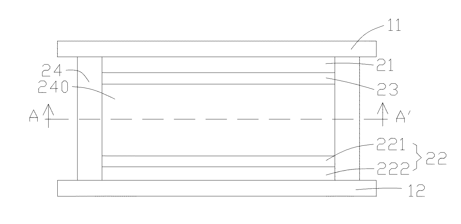
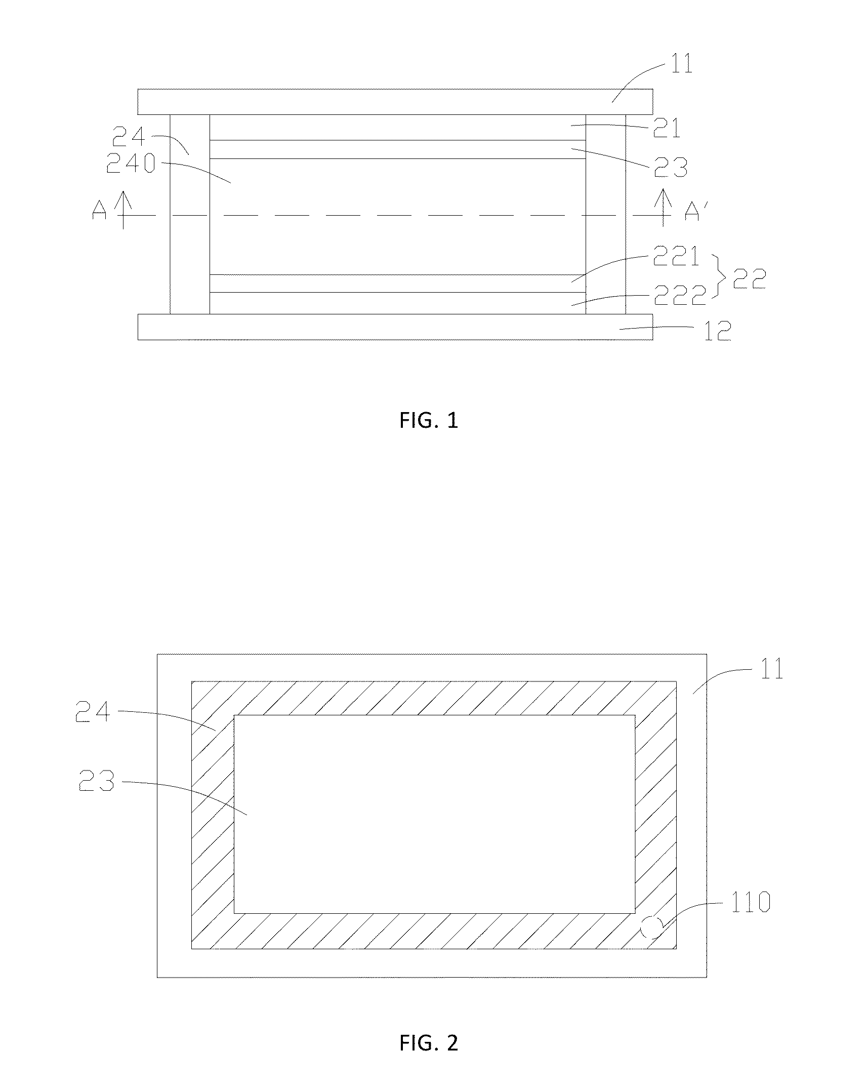
[0027]Referring to FIGS. 1 and 2, wherein FIG. 1 is an illustrational and configuration view of a field emitting light source made in accordance with the present invention; and FIG. 2 is a cross sectional view of the field emitting light source taken along line A-A′ of FIG. 1.

[0028]In the actual embodiment, the field emitting light source can be incorporated within a backlight module or other equipment in which a light source is needed. No limitations should be imposed herewith.

[0029]The field emitting light source includes, but not limited thereto, a first substrate 11, a second substrate 12, a second electrode layer 22, a light emitting layer 23, and a contained isolation layer 24.

[0030]The first substrate 11 can be made from ordinary glass, a clear glass, or as super clear glass or any other harder and transparent material. In the current embodiment, a comparably cost-effective clear glass is used which satisfies requirements of lower absorption and high penetration rate (more th...


PUM


Abstract

The present invention discloses a display device, a backlight module, and a first emitting light source. The light emitting light source includes first and second substrates arranged relatively with each other. A first electrode layer is formed on an internal side of the first substrate; and a second electrode layer is formed on an internal side of the second substrate. An light-emitting layer is arranged between the first and second transparent conductive layers, and formed over the first transparent conductive layer, wherein the light-emitting layer includes a quantum dot material. And wherein the second transparent conductive layer is used to emit electrons toward the light emitting layer so as to create illumination for being used in is backlight module. A quantum dot material is incorporated so as to increase the light emitting performance of the light emitting light source.

Description

FIELD OF THE INVENTION[0001]The present invention relates to a technical field of display, and more particularly to a field emission on light source for use with the display. The present invention further relates to a backlight module incorporated with the field emission light source, and a display device built with such a backlight module.BACKGROUND OF THE INVENTION[0002]Even since the introduction of the liquid crystal display device with its featured quality of clear, compact, low energy consumption, and prolonged service life, it has become the mainstream of the display device.[0003]Normally, the liquid crystal display device needs a backlight module to illuminate the liquid crystal display such that the image display thereon can been clearly seen. In the past, the cold cathode fluorescent lamp (CCFL) and the light emitting diode (LED) have been selected as the light source of the backlight module. The CCFL features a light source as it has a light tube, while the LED is a spot ...

Claims


Application Information

Patent Timeline
IPC IPC(8): F21V33/00
CPCF21V33/00G02F1/133G02F1/133602H01J63/06H01J2201/30496H01J2201/30469H01J63/04H01J1/304H01J63/02H01J2201/30434
Inventor WANG, YEWEN
Owner SHENZHEN CHINA STAR OPTOELECTRONICS TECH CO LTD
Learn More