
Electronic devices with flexible display and method for manufacturing the same

a technology of electronic devices and flexible substrates, applied in thermoelectric devices, final product manufacturing, basic electric elements, etc., can solve the problems of increasing mechanical stress on the bent portion of the flexible substrate, affecting the various components on the bent portion, and inconvenient manufacturing of the same, so as to reduce the size of the display portion

Active Publication Date: 2014-08-07
LG DISPLAY CO LTD
View PDF3 Cites 286 Cited by
  • Summary
  • Abstract
  • Description
  • Claims
  • Application Information

AI Technical Summary

Benefits of technology

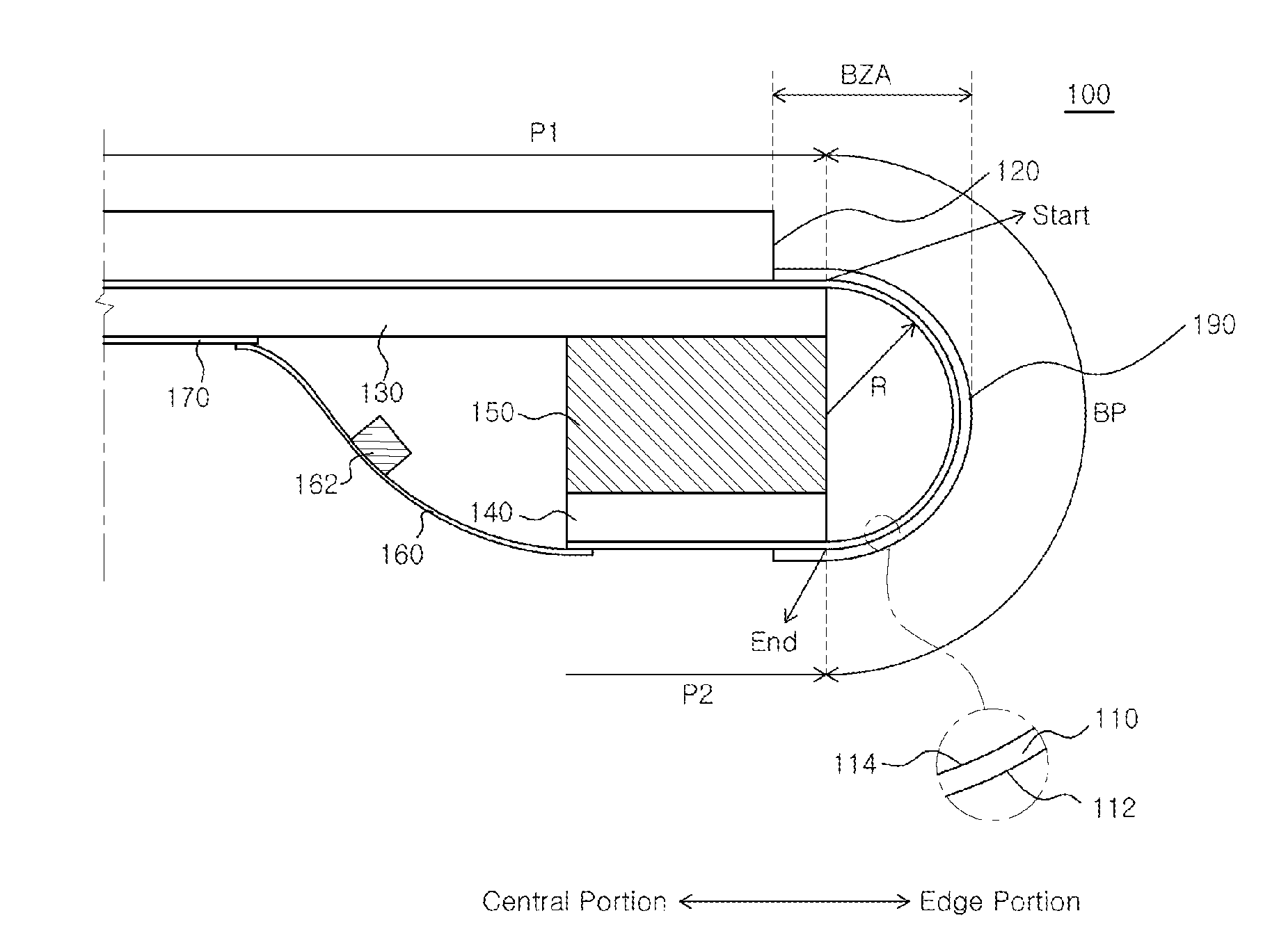
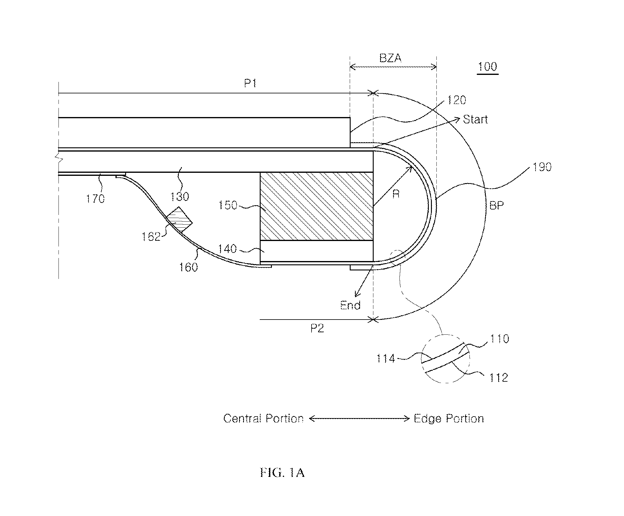
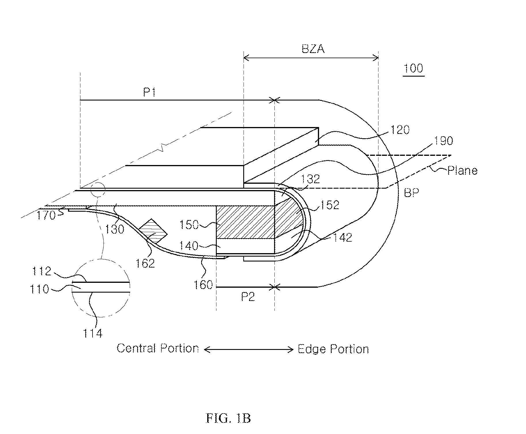
This patent describes an improved flexible display for electronic devices. The display has a flexible substrate with a curved edge that reduces the size of the bezel, or the area around the display. The substrate has two parts, with a space in between them. A support film is placed between two support films, and an insert member is used to reduce stress on the flexible substrate and its circuitry. This results in a more durable and efficient flexible display that minimizes the size of the bezel.

Problems solved by technology

However, inventors of the embodiments described herein have recognized that the support films at the inner side of the flexible substrate create several undesired side effects.
The force required to bend both the flexible substrate and the support film often result in excess mechanical stress to the bent portion of the flexible substrate.
Also, the increased mechanical stress may also affect the various components on the bent portion, for example, wires and insulation layer, and generate cracks or fractures.
In addition, the flexible substrate with the support film at the bent edge portion has a tendency to return to its original flat shape.
This tendency can cause the bent portion to become separated from a mounting structure to which it is adhered.
The tendency to go back to the original state may also exert an undesired force on various components or structures in the electronic device.

Method used


Image

  • Electronic devices with flexible display and method for manufacturing the same
  • Electronic devices with flexible display and method for manufacturing the same
  • Electronic devices with flexible display and method for manufacturing the same

Examples


Embodiment Construction

[0036]Various features and advantages described in the present disclosure will be more clearly understood from the following description with reference to the accompanying drawings. Note that the accompanying drawings are merely illustrative and may not be drawn to scale for easier explanation. Also, components having the same or similar function may be denoted by the corresponding reference symbols / numerals throughout the drawings for describing various embodiments. The corresponding reference numerals, for example, 110, 210, 310 and so on indicate the same elements throughout the specification. The descriptions of the same or similar components may be omitted.

[0037]It will be understood that when an element as a layer, region or substrate is referred to as being “on” or “over” another element, it can be directly on the other element or intervening elements may also be present. In contrast, when an element is referred to as being “directly on” or “directly over” another element, th...


PUM


Abstract

Embodiments of the present disclosure can significantly reduce the non-display area of a flexible OLED display, which would otherwise be covered by a cosmetic trim such as a bezel or an opaque. As such, an electronic device with a display having minimized border area can be provided. This makes it possible to reduce the overall size of the electronic device without sacrificing the size of the display therein. Such a reduction in size of the bezel was achieved by bending the flexible substrate near its edge using an insert member.

Description

CROSS-REFERENCE TO RELATED APPLICATIONS[0001]This application claims priority under 35 U.S.C. §119(e) to U.S. Provisional Patent Application No. 61 / 760,017 filed on Feb. 1, 2013 and under 35 U.S.C. §119 (a) to Korean Patent Application No. 10-2013-0147463 filed on Nov. 29, 2013, the disclosures of which are incorporated herein by reference.BACKGROUND OF THE INVENTION[0002]1. Technical Field[0003]This relates generally to electronic devices, and more particularly, to displays for electronic devices.[0004]2. Description of the Related Art[0005]Electronic devices often include displays to present information for a user. Such displays are often made from rigid display structures with large non-display area to accommodate circuitry necessary for operating display pixels in a display area of the display. In some displays, the width of the non-display area reaches up to a centimeter wide or more. Such a wide non-display area tends to make displays bulky, which in turn, necessitates use of ...

Claims


Application Information

Patent Timeline
Patent Type & Authority Applications(United States)
IPC IPC(8): H01L27/32H01L51/56H10K99/00
CPCH01L51/56H01L27/326Y02E10/549Y02P70/50H10K59/10H10K77/111H10K59/8722H10K50/8426
Inventor KWON, SEYEOULYOO, JUHN SUKYANG, JAE HUNYANG, HEESEOKLEE, CHANWOOYOUN, SANGCHEONJO, SOYOUNG
Owner LG DISPLAY CO LTD
Learn More