Supercharge Your Innovation With Domain-Expert AI Agents!

Methods for manufacturing integrated circuit devices having features with reduced edge curvature

a technology of integrated circuit devices and features, applied in the direction of cad circuit design, computer aided design, instruments, etc., can solve the problems of reducing yield, systematic and random deviation of the etched shape of features from the desired shape, and manufacturing devices with very small features, so as to achieve tighter straightening of sidewall surfaces and improve line definition

Active Publication Date: 2014-08-07
SYNOPSYS INC
View PDF21 Cites 6 Cited by
  • Summary
  • Abstract
  • Description
  • Claims
  • Application Information

AI Technical Summary

Benefits of technology

This approach results in significantly reduced line edge roughness and corner rounding, achieving straighter edges and sharper corners with variations controlled within a tighter distribution than conventional lithographic techniques, enhancing the performance and yield of integrated circuit devices.

Problems solved by technology

One problem associated with manufacturing devices having very small features arises because of variations introduced by the photolithographic processes.
Specifically, resist material properties, process conditions, optical distortions and other factors can cause systematic and random deviations in the etched shapes of the features from their desired shapes.
As process technologies continue to shrink, these deviations become a greater percentage of the critical dimension of the etched lines, which can reduce yield and result in significant performance variability in devices such as transistors implemented utilizing these etched lines.

Method used


Image

  • Methods for manufacturing integrated circuit devices having features with reduced edge curvature
  • Methods for manufacturing integrated circuit devices having features with reduced edge curvature
  • Methods for manufacturing integrated circuit devices having features with reduced edge curvature

Examples


Embodiment Construction

[0019]The following description is presented to enable any person skilled in the art to make and use the invention, and is provided in the context of a particular application and its requirements. Various modifications to the disclosed embodiment will be readily apparent to those skilled in the art, and the general principles defined herein may be applied to other embodiments and applications without departing from the spirit and scope of the present invention. Thus, the present invention is not intended to be limited to the embodiments shown, but is to be accorded with the widest scope consistent with the principles and features disclosed herein.

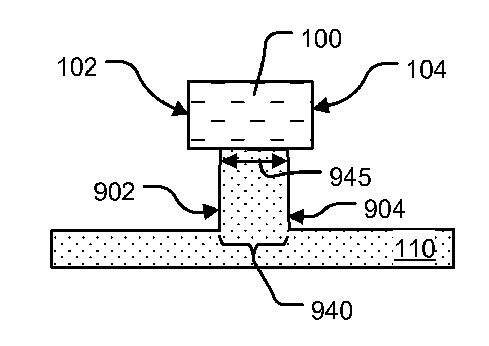
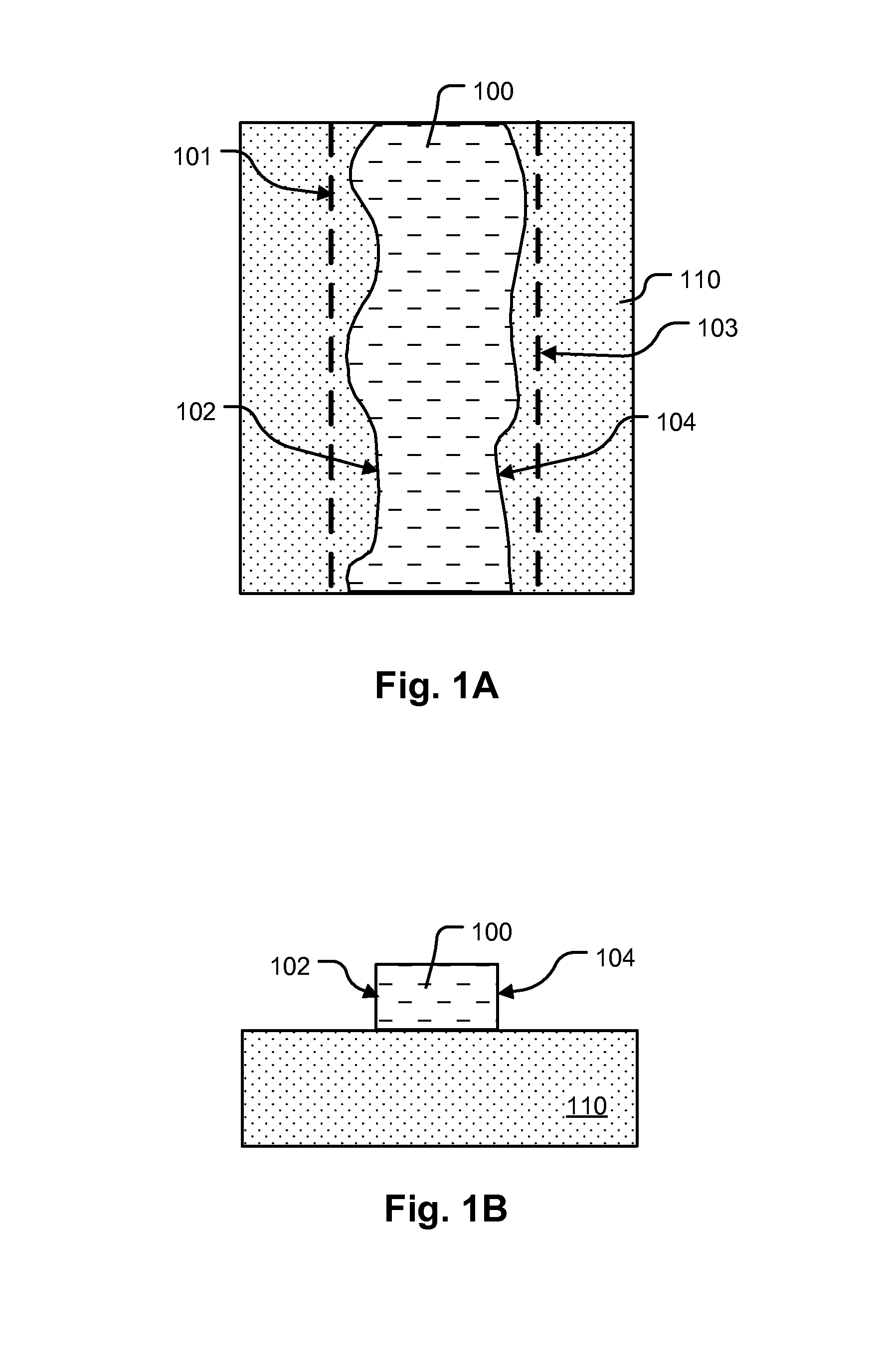
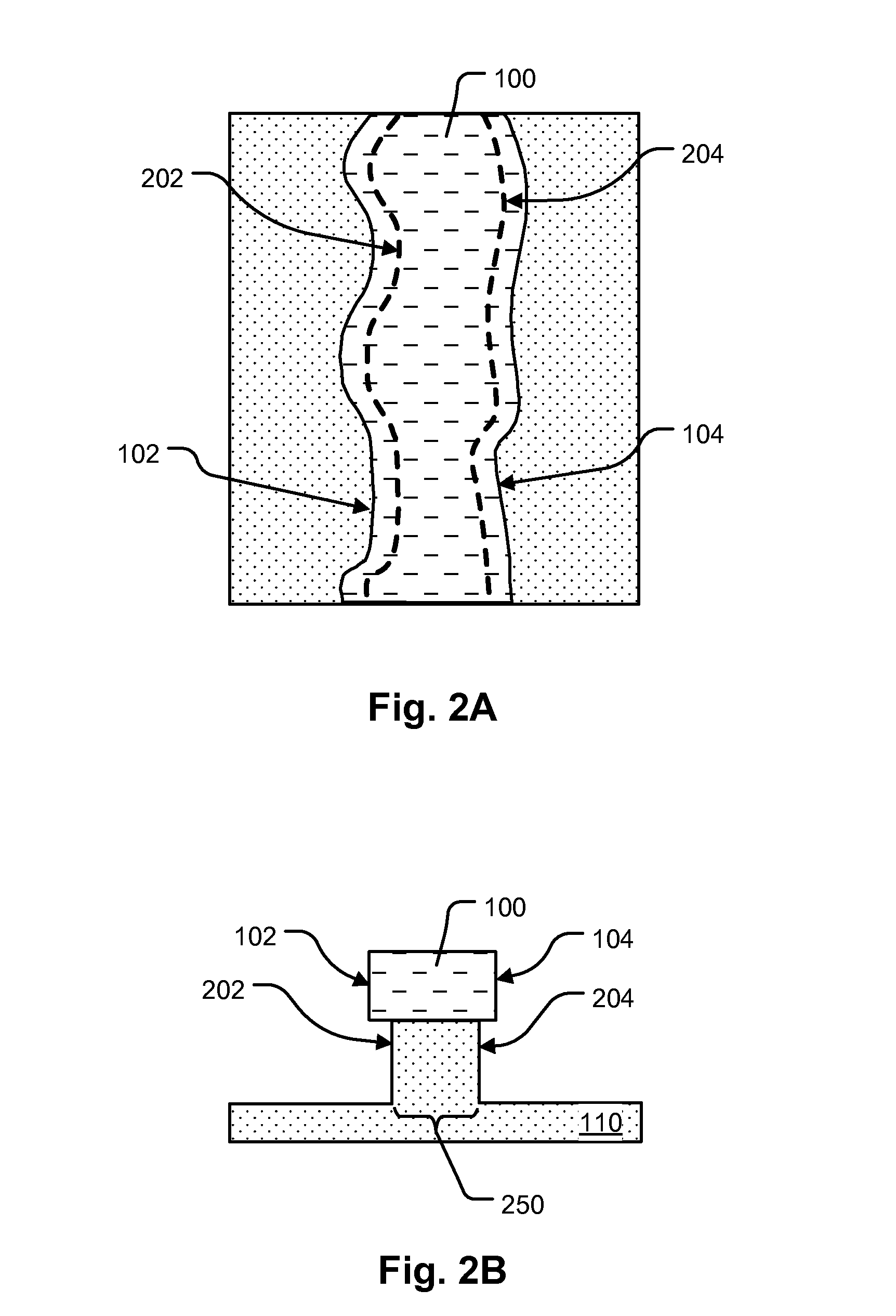
[0020]FIGS. 1-4 illustrate stages in a manufacturing process flow of an embodiment for straightening an etched sidewall surface of a line of crystalline phase material. It will be understood that the process steps and structures described with reference to FIGS. 1-4 do not describe a complete process for the manufacturing of an integrated c...


PUM


Abstract

A structure, such as an integrated circuit device, is described that includes a line of material with critical dimensions which vary within a distribution substantially less than that of a mask element, such as a patterned resist element, used in etching the line. Techniques are described for processing a line of crystalline phase material which has already been etched using the mask element, in a manner which straightens an etched sidewall surface of the line. The straightened sidewall surface does not carry the sidewall surface variations introduced by photolithographic processes, or other patterning processes, involved in forming the mask element and etching the line.

Description

CROSS-REFERENCE TO RELATED APPLICATIONS[0001]The present application is a Continuation of PCT International Application No. PCT / US12 / 54224, entitled “METHODS FOR MANUFACTURING INTEGRATED CIRCUIT DEVICES HAVING FEATURES WITH REDUCED EDGE CURVATURE,” by Victor Moroz and Lars Bomholt, filed 7 Sep. 2012, which application claims the benefit of U.S. patent application Ser. No. 13 / 350,523, entitled “METHODS FOR MANUFACTURING INTEGRATED CIRCUIT DEVICES HAVING FEATURES WITH REDUCED EDGE CURVATURE,” by Victor Moroz and Lars Bomholt, filed 13 Jan. 2012, which application is a non-provisional of U.S. Provisional Application No. 61 / 532,475 entitled “CRYSTAL SELF-ASSEMBLY APPLIED TO FEATURE PATTERNING,” by Victor Moroz and Lars Bomholt, filed 8 Sep. 2011. All the above applications are incorporated herein by reference.BACKGROUND[0002]1. Field of the Invention[0003]The present invention relates to integrated circuit fabrication, and more particularly to methods for fabricating high-density integr...

Claims


Application Information

Patent Timeline
Patent Type & Authority Applications(United States)
IPC IPC(8): G06F17/50
CPCG06F17/5045H01L21/02612H01L21/02656H01L21/30608H01L21/3065H01L21/0274H01L29/045H01L29/0676G06F30/30H01L21/308
Inventor MOROZ, VICTORBOMHOLT, LARS
Owner SYNOPSYS INC
Features
  • R&D
  • Intellectual Property
  • Life Sciences
  • Materials
  • Tech Scout
  • Unparalleled Data Quality
  • Higher Quality Content
  • 60% Fewer Hallucinations
Learn More