Eureka AIR delivers breakthrough ideas for toughest innovation challenges, trusted by R&D personnel around the world.

Methods for manufacturing integrated circuit devices having features with reduced edge curvature

Active Publication Date: 2013-03-14
SYNOPSYS INC
View PDF2 Cites 1 Cited by
  • Summary
  • Abstract
  • Description
  • Claims
  • Application Information

AI Technical Summary

Benefits of technology

This patent describes a technique for controlling the smoothness of the sidewalls of a line of material made using a mask. The technique results in a smoother, more definitive line than can be achieved using traditional methods. The straightened line of material also has improved edge roughness, with results showing less than 1 nm of roughness.

Problems solved by technology

One problem associated with manufacturing devices having very small features arises because of variations introduced by the photolithographic processes.
Specifically, resist material properties, process conditions, optical distortions and other factors can cause systematic and random deviations in the etched shapes of the features from their desired shapes.
As process technologies continue to shrink, these deviations become a greater percentage of the critical dimension of the etched lines, which can reduce yield and result in significant performance variability in devices such as transistors implemented utilizing these etched lines.

Method used


Image

  • Methods for manufacturing integrated circuit devices having features with reduced edge curvature
  • Methods for manufacturing integrated circuit devices having features with reduced edge curvature
  • Methods for manufacturing integrated circuit devices having features with reduced edge curvature

Examples


Embodiment Construction

[0020]The following description is presented to enable any person skilled in the art to make and use the invention, and is provided in the context of a particular application and its requirements. Various modifications to the disclosed embodiment will be readily apparent to those skilled in the art, and the general principles defined herein may be applied to other embodiments and applications without departing from the spirit and scope of the present invention. Thus, the present invention is not intended to be limited to the embodiments shown, but is to be accorded with the widest scope consistent with the principles and features disclosed herein.

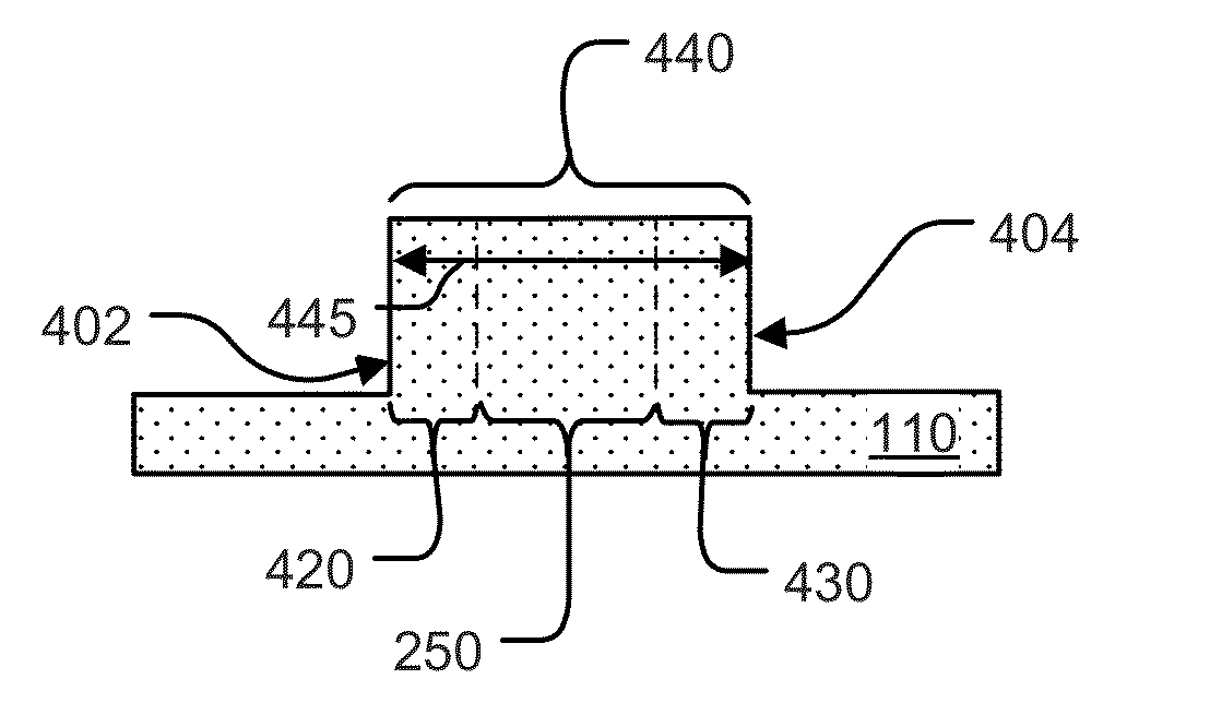
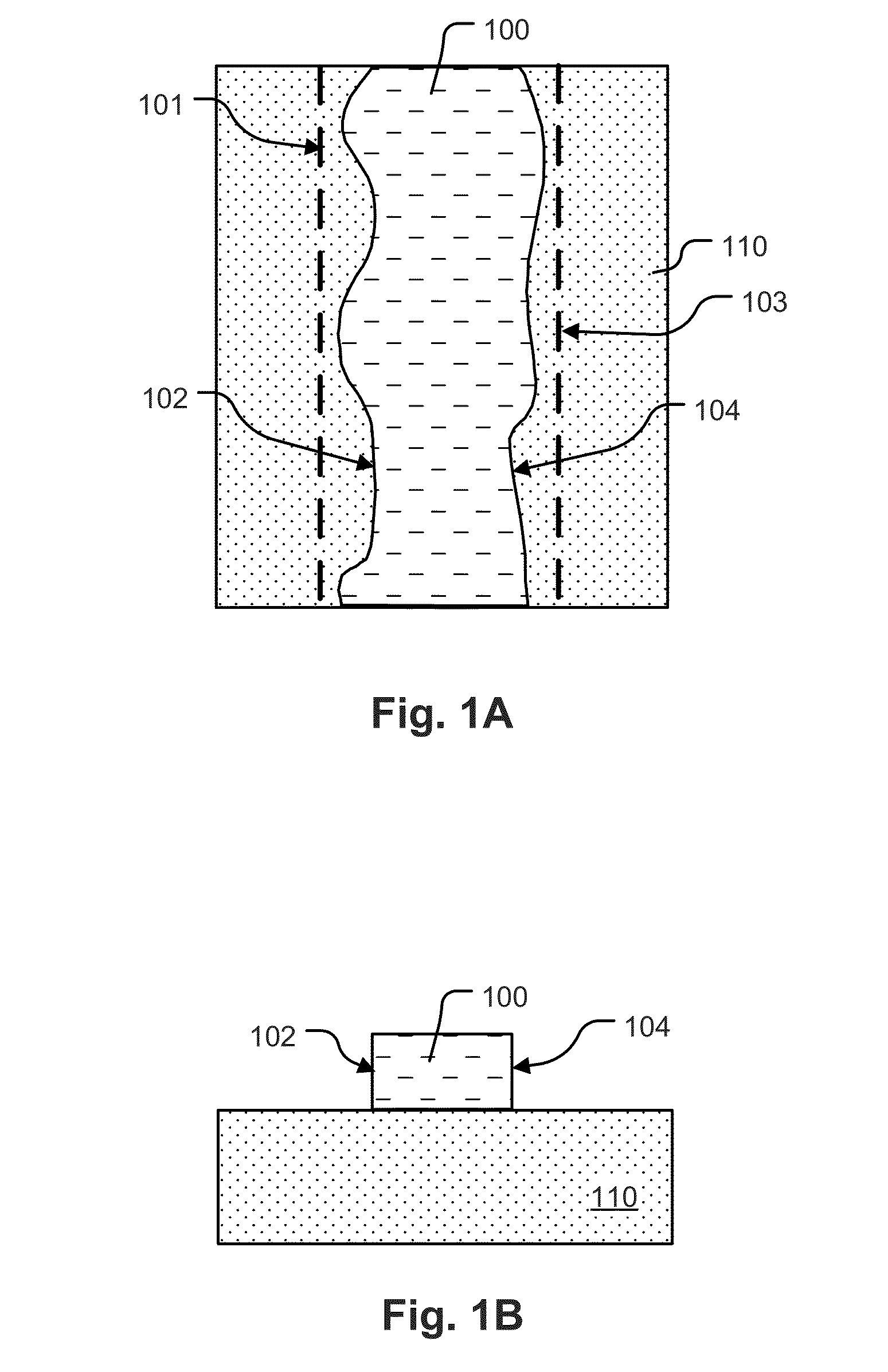
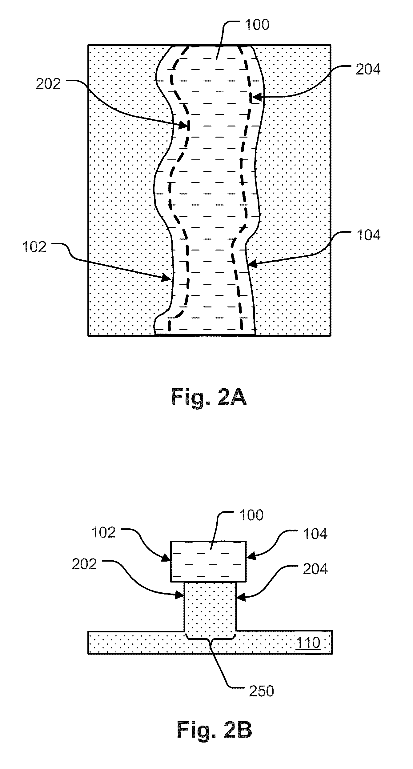
[0021]FIGS. 1-4 illustrate stages in a manufacturing process flow of an embodiment for straightening an etched sidewall surface of a line of crystalline phase material. It will be understood that the process steps and structures described with reference to FIGS. 1-4 do not describe a complete process for the manufacturing of an integrated c...


PUM


Abstract

A structure, such as an integrated circuit device, is described that includes a line of material with critical dimensions which vary within a distribution substantially less than that of a mask element, such as a patterned resist element, used in etching the line. Techniques are described for processing a line of crystalline phase material which has already been etched using the mask element, in a manner which straightens an etched sidewall surface of the line. The straightened sidewall surface does not carry the sidewall surface variations introduced by photolithographic processes, or other patterning processes, involved in forming the mask element and etching the line.

Description

CROSS-REFERENCE TO RELATED APPLICATIONS[0001]The present application claims the benefit of U.S. Provisional Application No. 61 / 532,475 entitled “Crystal Self-Assembly Applied to Feature Patterning” filed 8 Sep. 2011, which is incorporated by reference herein.[0002]U.S. application Ser. No. 13 / 190,319 entitled “Integrated Circuit Devices having Features with Reduced Edge Curvature and Methods for Manufacturing the Same” filed 25 Jul. 2011, is incorporated by reference herein.BACKGROUND[0003]1. Field of the Invention[0004]The present invention relates to integrated circuit fabrication, and more particularly to methods for fabricating high-density integrated circuit devices.[0005]2. Description of Related Art[0006]Photolithographic processes can be used to form a variety of integrated circuit structures on a semiconductor wafer. In photolithography, features of these structures are typically created by exposing a mask pattern (or reticle) to project an image onto a wafer that is coated...

Claims


Application Information

Patent Timeline
IPC IPC(8): H01L21/20H01L21/302
CPCH01L21/30608G06F17/5045H01L21/3065H01L21/02612H01L21/02656H01L21/0274H01L29/045H01L29/0676G06F30/30H01L21/308
Inventor MOROZ, VICTORBOMHOLT, LARS
Owner SYNOPSYS INC
Why Eureka
Eureka Blog
Learn More