Eureka AIR delivers breakthrough ideas for toughest innovation challenges, trusted by R&D personnel around the world.

Semiconductor device with multiple carrier channels

Active Publication Date: 2016-08-16
MITSUBISHI ELECTRIC RES LAB INC
View PDF8 Cites 15 Cited by
  • Summary
  • Abstract
  • Description
  • Claims
  • Application Information

AI Technical Summary

Benefits of technology

The patent describes an invention that provides an electrode structure for a semiconductor device that allows direct control over each channel. This structure enables the use of multiple channels without compromising the gate width. The electrodes are interdigitated, meaning that they are arranged in a way that their fingers meet, which helps to enhance current flow and improve the device's performance. The method for fabricating this structure can be used for different types of semiconductor devices, such as transistors and power amplifiers. The technical effects of this invention include better performance and control over semiconductor devices with multiple channels.

Problems solved by technology

However, the limited breakdown voltage and frequency response of Si, and its higher resistance make the commercial devices and circuits currently available very bulky, heavy and inappropriate for future power applications.
For GaN-based power devices, although the device breakdown voltage can increase with increasing gate-to-drain distance, the Imax is currently limited by the transport capability of the single channel, where I saturates at high electric field due to the saturation of carrier mobility and velocity and the alleviated channel temperature.
In AlGaN / GaN HEMTs, double-channel structures can not only enable a high output current, but also reduce the differential source access resistance for higher linearity and gain cutoff frequency.
However, the double-channel structure of HEMTs, although delivered a higher drain current density, can have large subthreshold swing, low threshold voltage, short-channel effects and non-linear gate transconductance, due to a weak gate control over the lower 2DEG channel.
The weak gate control not only harms the benefits of double-channel device in current enhancement, but inhibits the development of multi-channel devices, as it is more difficult for gate to turn on or off more channels below the first channel.
However, the transfer characteristics of the double-channel HEMTs with back-barrier are still much inferior to that of single-channel HEMTs.
However, this solution sacrifices the gate width, making only ˜½ gate width actually usable, which greatly reduced the effective current density (total current over total device width) and therefore loses the advantage of current enhancement brought by multi-channels.
On the other hand, as current needs to aggregate into the regions between the spaced apart gates, current crowding and electric field crowding near the gate is inevitable, which would typically lead to high channel temperature, preliminary device breakdown and poor device reliability.

Method used


Image

  • Semiconductor device with multiple carrier channels
  • Semiconductor device with multiple carrier channels
  • Semiconductor device with multiple carrier channels

Examples


Embodiment Construction

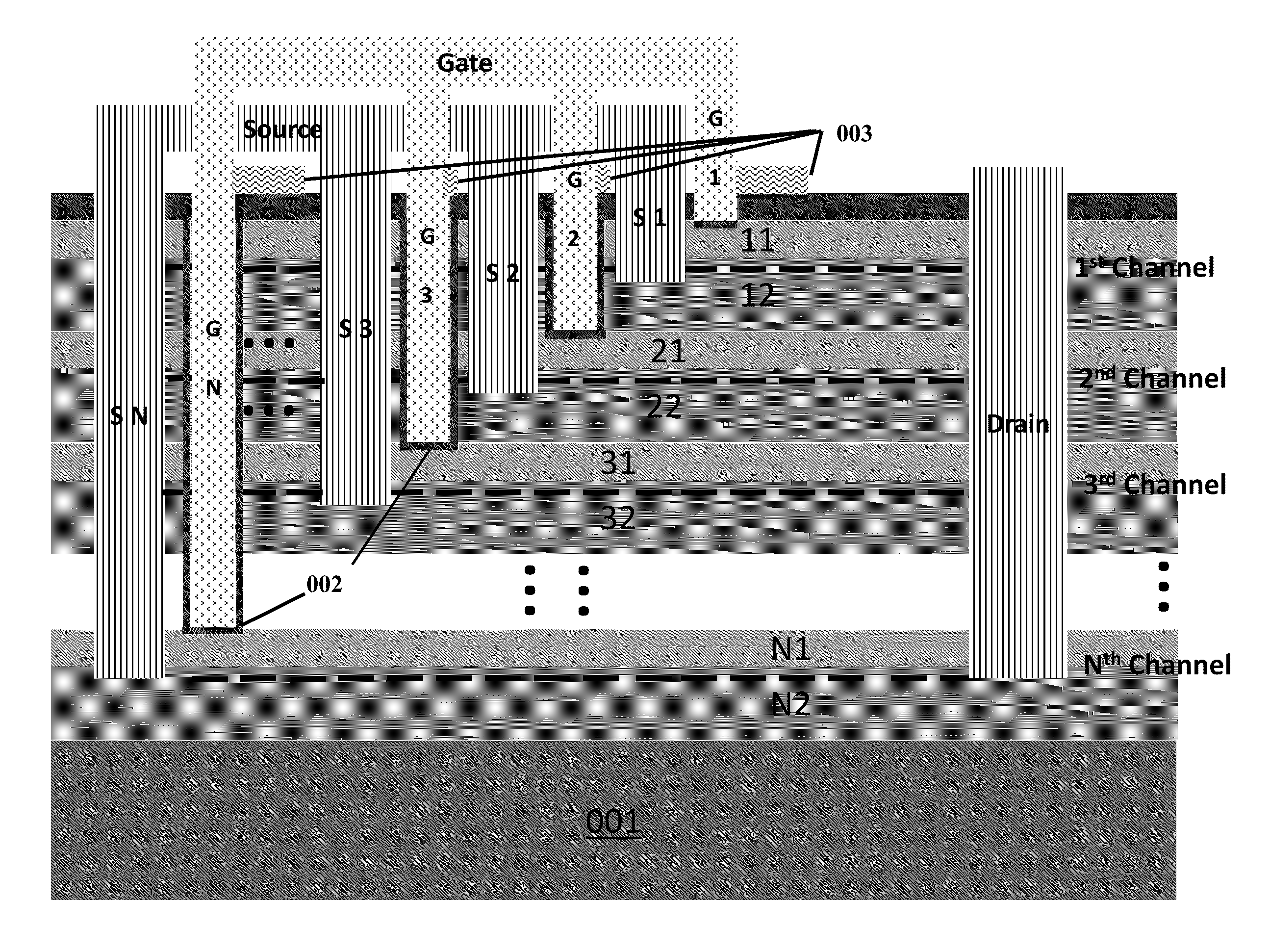
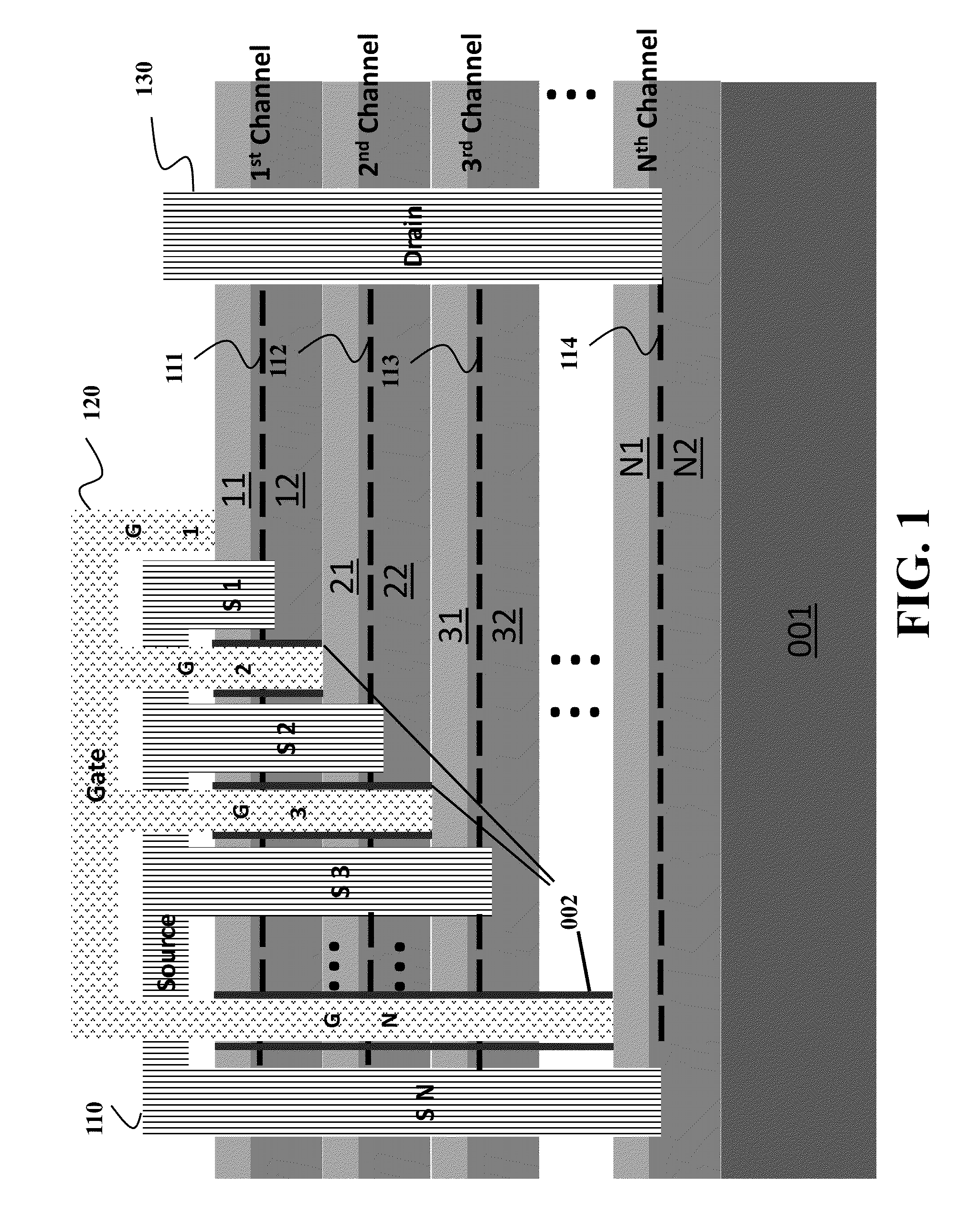
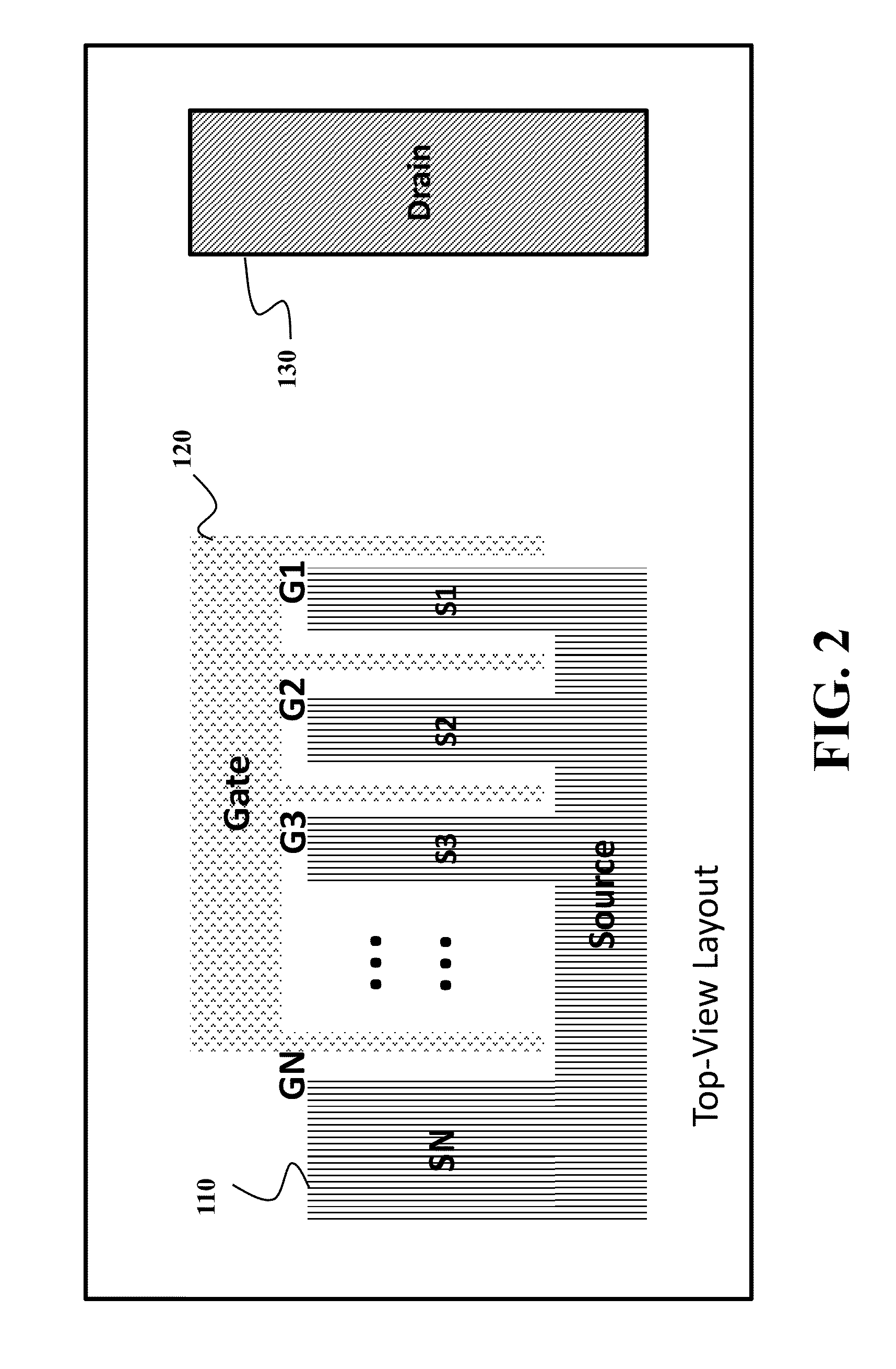
[0023]Various embodiments of the invention relates to a semiconductor device with multi-channels structure and an electrode controlling the multi-channels, and the methods and techniques for fabricating the device. Merely by way of example, different embodiments can be applied to methods and systems for manufacturing semiconductor devices with multiple two-dimensional-electron (2DEG) channels and / or two-dimensional-hole (2DHG) channels. The methods and techniques can be applied to a variety of three-terminal semiconductor devices, including but not limiting to bipolar transistors, field-effect transistor, insulated-gate bipolar transistors (IGBTs), and thyristors to enable the control over multi-channels in the device. The principles employ by some embodiments of the invention can be also used to form and / or fabricate the multi-channel field effect transistor (FET).

[0024]FIG. 1 shows a simplified cross-sectional diagram of a semiconductor device according to one embodiment of the in...


PUM


Abstract

A semiconductor device includes a layered structure forming multiple carrier channels extending in parallel at different depths of the semiconductor device and a gate electrode having multiple gate fingers of different lengths penetrating the layered structure to reach and control corresponding carrier channels at the different depths. The semiconductor device also includes a carrier electrode having multiple carrier fingers of different lengths penetrating the layered structure to access the corresponding carrier channels. The carrier fingers are interdigitated with the gate fingers.

Description

RELATED APPLICATION[0001]This application claims priority from a provisional application 62 / 193,673 filed on Jul. 17, 2015 and incorporated herein by reference.FIELD OF THE INVENTION[0002]The present invention relates generally to semiconductor device, and more particularly to semiconductor devices with multiple carrier channels.BACKGROUND OF THE INVENTION[0003]Semiconductor devices play a significant role in solving the energy challenges. Specifically, nitride power transistors have great potential in the application of advanced transportation systems, more robust energy delivery networks and many new revolutionary approaches to high-efficiency electricity generation and conversion. Those systems rely on very efficient converters to step-up or step-down electric voltages. Nowadays, these devices are mainly made of silicon (Si). However, the limited breakdown voltage and frequency response of Si, and its higher resistance make the commercial devices and circuits currently available ...

Claims


Application Information

Patent Timeline
IPC IPC(8): H01L29/778H01L29/20H01L29/205H01L29/423H01L29/417H01L29/40H01L29/66
CPCH01L29/7784H01L29/2003H01L29/205H01L29/4238H01L29/41758H01L29/404H01L29/66462H01L29/7783H01L29/7781H01L29/778H01L29/7782H01L29/66431H01L29/7788H01L29/7789H01L29/41766H01L29/42316H01L29/4236H01L29/0843H01L29/402
Inventor TEO, KOON HOOZHANG, YUHAO
Owner MITSUBISHI ELECTRIC RES LAB INC
Why Eureka
Eureka Blog
Learn More