Resistive switching device for a non-volatile memory device

Inactive Publication Date: 2014-08-14
CROSSBAR INC
View PDF4 Cites 1 Cited by
  • Summary
  • Abstract
  • Description
  • Claims
  • Application Information

AI Technical Summary

Benefits of technology

[0009]In an embodiment, a method for forming a semiconductor device including a resistive memory cell includes providing a substrate having an upper surface. A first conductive layer is formed over the upper surface of the substrate. An amorphous silicon layer is formed over the first conductive layer. A surface of the amorphous silicon layer is cleaned to remove native oxide formed on the surface of the amorphous silicon layer. A silver layer is deposited over the amorphous silicon layer after removing the native oxide by performing the cleaning step. The memory cell includes the first conductive layer, the amorphous silicon layer, and the second conductive layer. The surface of the amorphous silicon layer is cleaned to prevent silver agglomeration on the native oxide.
[0010]In an embodiment, the cleaning step includes sputtering using an inert gas or dipping the substrate having the amorphous silicon layer in a solution including hydrogen fluoride. The silver layer may be formed to a thickness of no more than 800 angstroms, or no more than 500 angstroms, or no more than 200 angstroms.
[0011

Problems solved by technology

In the case of a-Si structures, electric field-induced diffusion of metal ions into the silicon

Method used


Image

  • Resistive switching device for a non-volatile memory device
  • Resistive switching device for a non-volatile memory device
  • Resistive switching device for a non-volatile memory device

Examples


Example

[0026]The present invention relates to methods for producing a smooth, continuous silver film on a semiconductor device, in particular on a resistive memory device.

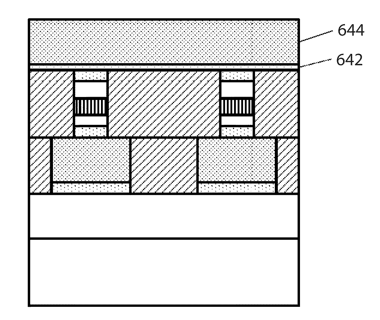
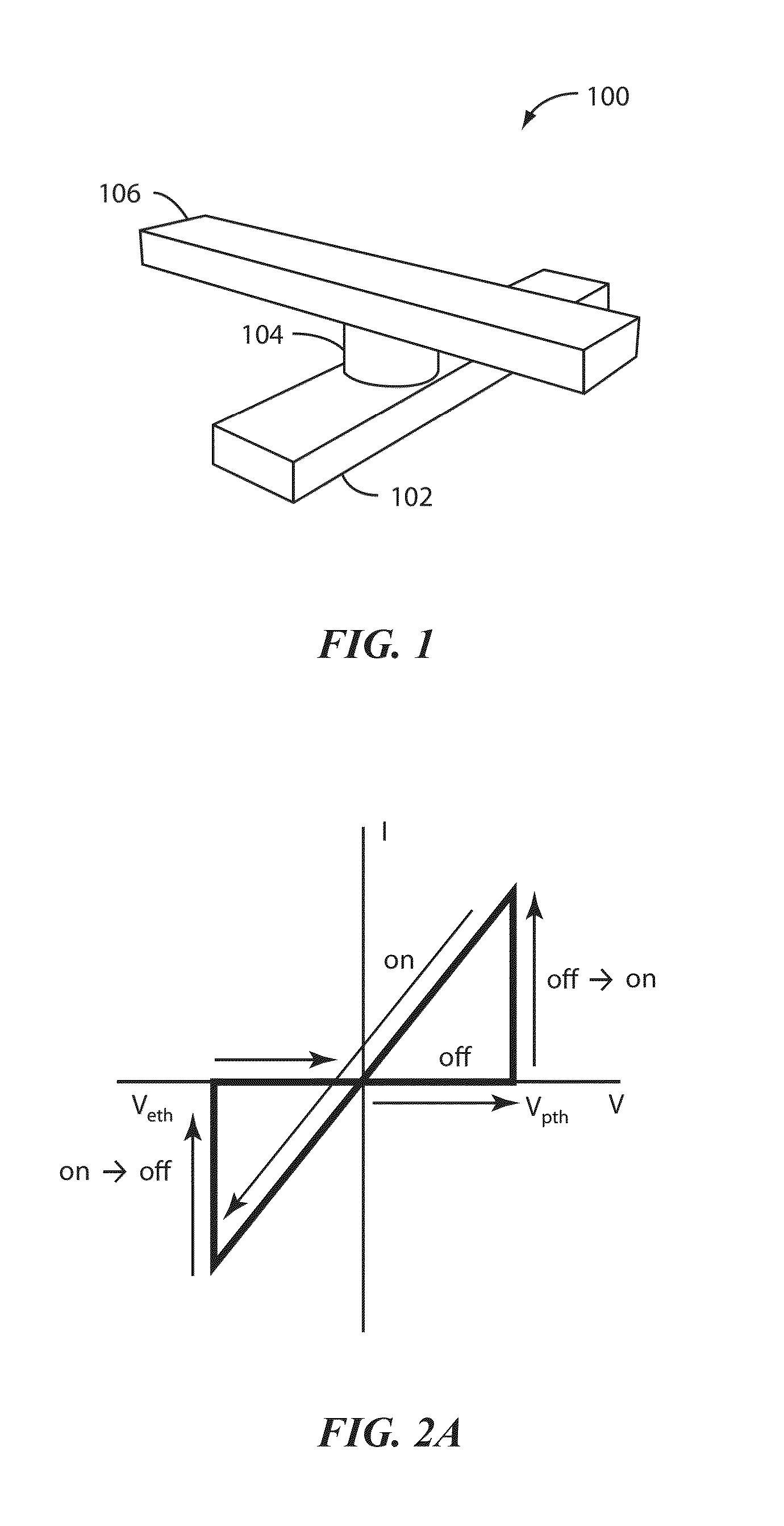
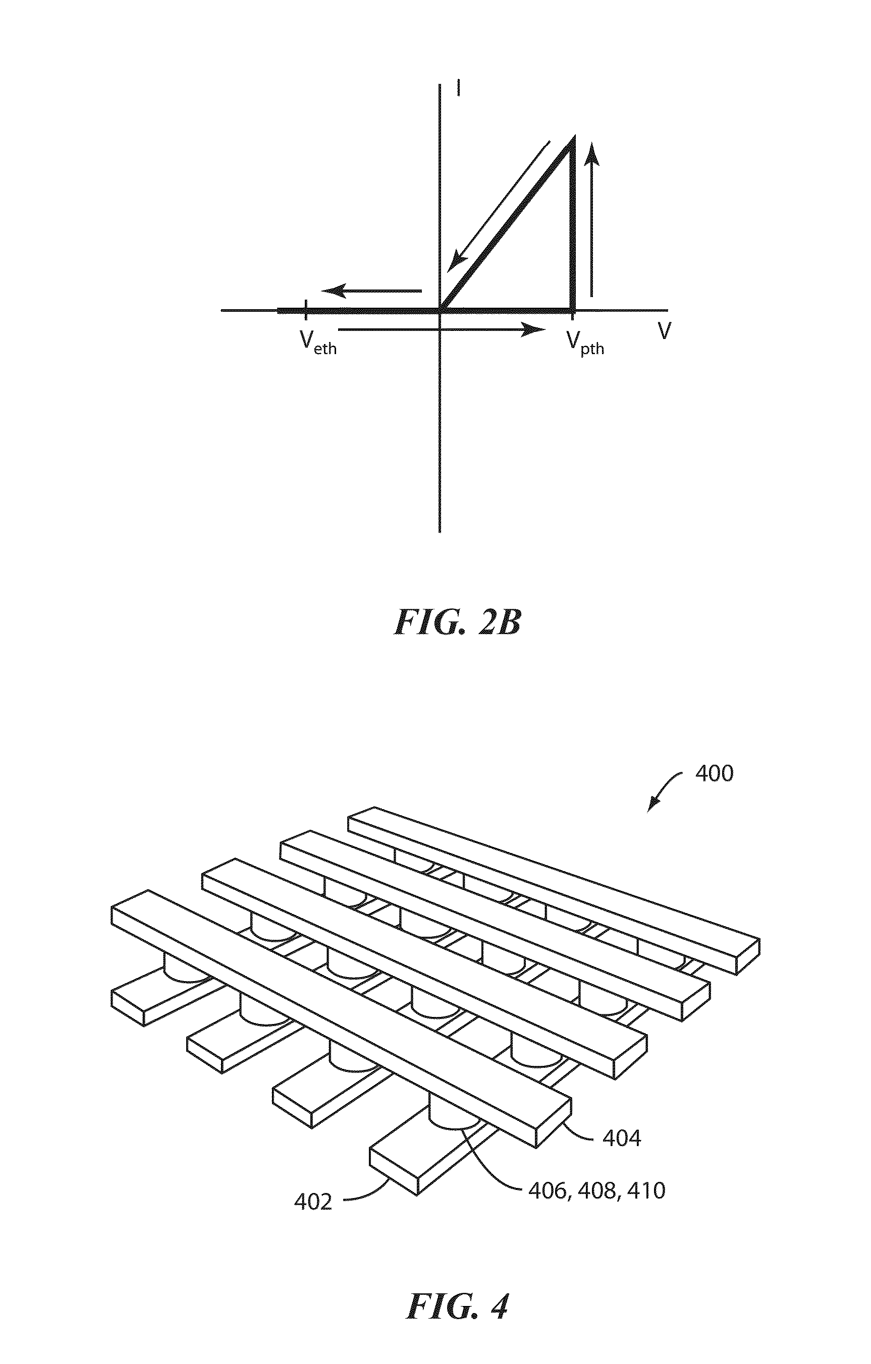
[0027]FIG. 1 illustrates a memory cell 100 in a non-volatile memory device, e.g., a semiconductor memory chip. The memory cell includes a bottom electrode 102, a switching medium 104, and a top electrode 106 according an embodiment of the present invention. The switching medium 104 exhibits a resistance that can be selectively set to various values, and reset, using appropriate control circuitry. The cell 100 is a two-terminal resistive memory device, e.g., resistive random-access memory (RRAM), in the present embodiment.

[0028]The resistive memory cell is a two-terminal memory cell having a switching medium provided between top and bottom electrodes. The resistance of the switching medium can be controlled by applying an electrical signal to the electrodes. The electrical signal may be current-based or voltage-based. As u...


PUM


Abstract

A method for forming a non-volatile memory device configured with a resistive switching element includes providing a substrate having a surface region, depositing a first dielectric material overlying the surface region, forming a first wiring structure overlying the first dielectric material, forming a contact layer of doped polycrystalline silicon containing material overlying the first wiring structure, forming a switching layer of resistive switching material over the contact layer, removing native oxide formed on a top surface of the switching layer, if any, depositing a metal layer of an active metal directly upon the top surface of the switching layer, and depositing a second wiring structure overlying the metal layer, wherein the top surface of the switching layer is cleaned of the native oxide, if any, to reduce agglomeration of the active metal.

Description

CROSS REFERENCE TO RELATED APPLICATIONS[0001]The present application is a continuation-in-part of U.S. application Ser. No. 13 / 461,725, filed May 1, 2012, now issued as U.S. Pat. No. 8,697,533, issue date: Apr. 15, 2014, which is a continuation of U.S. application Ser. No. 12 / 913,719, filed Oct. 27, 2010, now issued as U.S. Pat. No. 8,187,945, issue date: May 29, 2012. The present application is also a continuation-in-part of U.S. application Ser. No. 14 / 034,390, filed Sep. 23, 2012, which is a continuation of U.S. application Ser. No. 13 / 585,759, filed Aug. 14, 2012, now issued as U.S. Pat. No. 8,569,172, issue date Oct. 29, 2013. These cited references are hereinby incorporated by reference for all purposesSTATEMENTS RELATED TO GOVERNMENT OR FEDERALLY FUNDED RESEARCH[0002]Not ApplicableBACKGROUND[0003]The present invention relates to a memory device including resistive memory cells, in particular methods for producing a smooth, continuous silver film on a semiconductor device, in ...

Claims


Application Information

Patent Timeline
IPC IPC(8): H01L45/00
CPCH01L45/1253H01L45/1608H10B63/80H10N70/245H10N70/826H10N70/8416H10N70/884H10N70/011H10N70/023H10N70/063
Inventor HERNER, SCOTT BRADJO, SUNG HYUN
Owner CROSSBAR INC
Why Eureka
Try Eureka