Methods of fabricating electronic and mechanical structures

a technology of electronic and mechanical structures and methods, applied in the direction of additive manufacturing processes, waveguides, manufacturing tools, etc., can solve the problems of limited use fields, and unfavorable direct 3d manufacturing

Inactive Publication Date: 2014-08-21
CUBIC CORPORATION
View PDF7 Cites 101 Cited by
  • Summary
  • Abstract
  • Description
  • Claims
  • Application Information

AI Technical Summary

Benefits of technology

[0024]FIGS. 1F and 1G schematically illustrate a method and resulting structure similar to that of FIGS. 1C-1D but having a sacrificial material 18 disposed on the second s...

Problems solved by technology

More and more components are being added to devices that are getting increasingly complex and smaller.
The ability to achieve customization in such devices and still allow them to be affordably manufactured has remained a challenge.
Still there are many fields where the ability to make custom 3D parts of heterogeneous materials has remained elusive and substantial sacrifices in dimensional accuracy and precision, material diversity, upward or downward size scaling, for example from microns to meters, and/or other limitations have relegated most direct 3D manufacturing to either be unaffordable, impractical, or find limited fields of use, for example to make plastic prototypes for novelty, engineering understanding, or marketing.
Alternatively, molding is used but is limited in the complexity of the parts and number that can be made and are usually of limited material diversity.
For example, one would not expect injection molding to make parts of plastic, metal, and ceramic in the same molding operation.
Furthermore, the use of PIDs to create such devices is very limiting.
After a layer of PID is imaged to form a structure, a second layer, uniformly applied from either a liquid or a dry film, has difficulty planarizing or filling the spaces in the structure particularly if they are on the scale of the layer's thickness or greater.
A further limitation is the inability to create structures of varying and specific desired thicknesses since the PID can only be applied as one uniform thickness when applied by these methods.
Still a further limitation is the inability of the PID to allow for selective metallization.
A still further limitation of the current techniques is the inability to create structures that differ substantially in size, functionality, and accuracy and also can provide the needed material diversity wherein the materials have both acceptable properties in comparison to other forming techniques currently known—for ...

Method used


Image

  • Methods of fabricating electronic and mechanical structures
  • Methods of fabricating electronic and mechanical structures
  • Methods of fabricating electronic and mechanical structures

Examples


Embodiment Construction

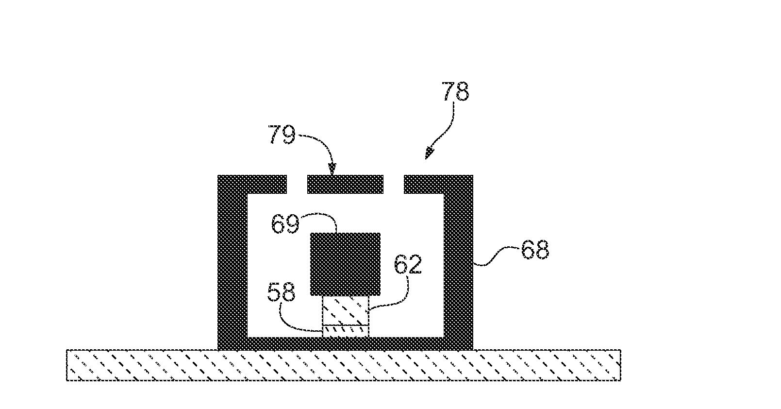
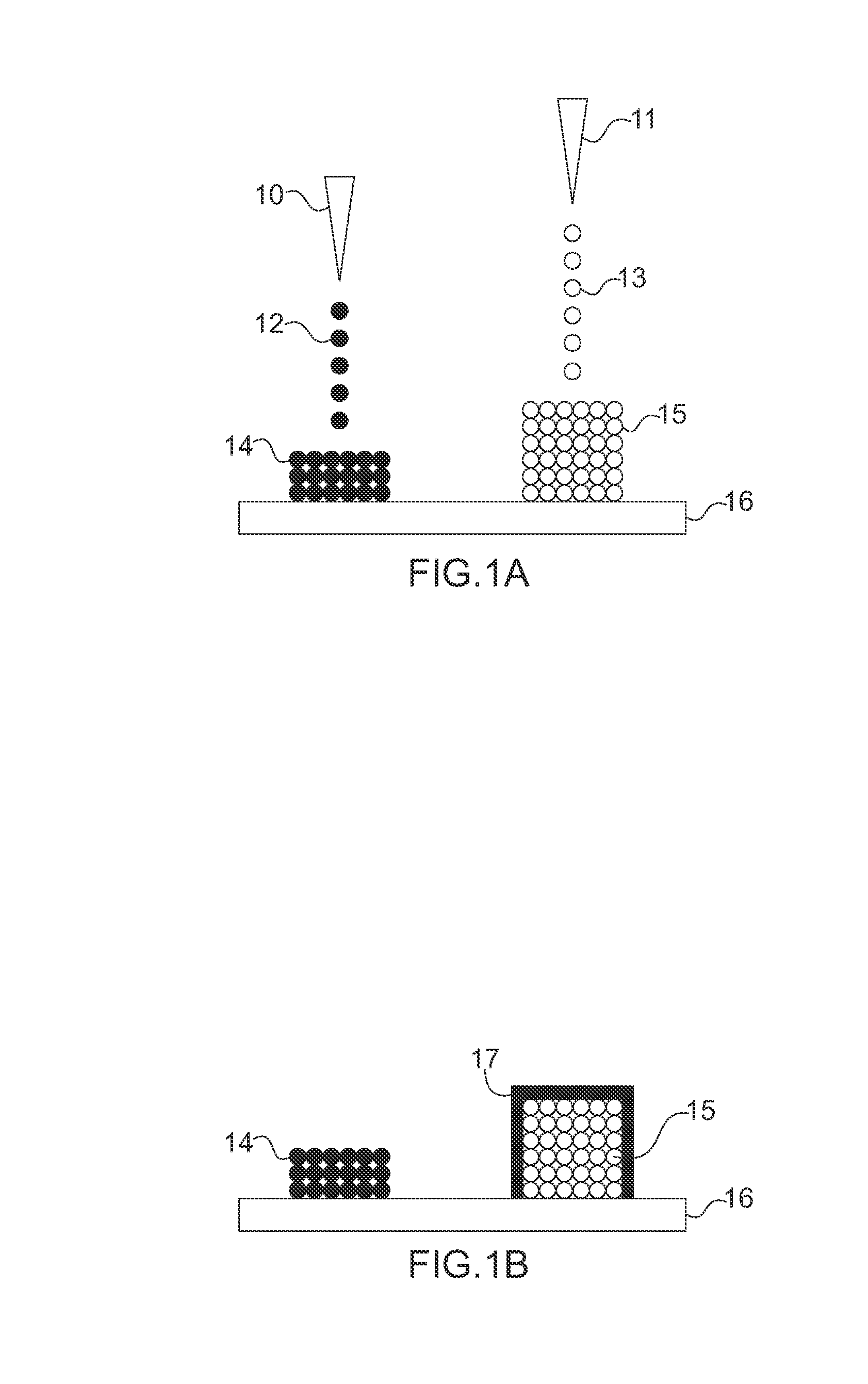
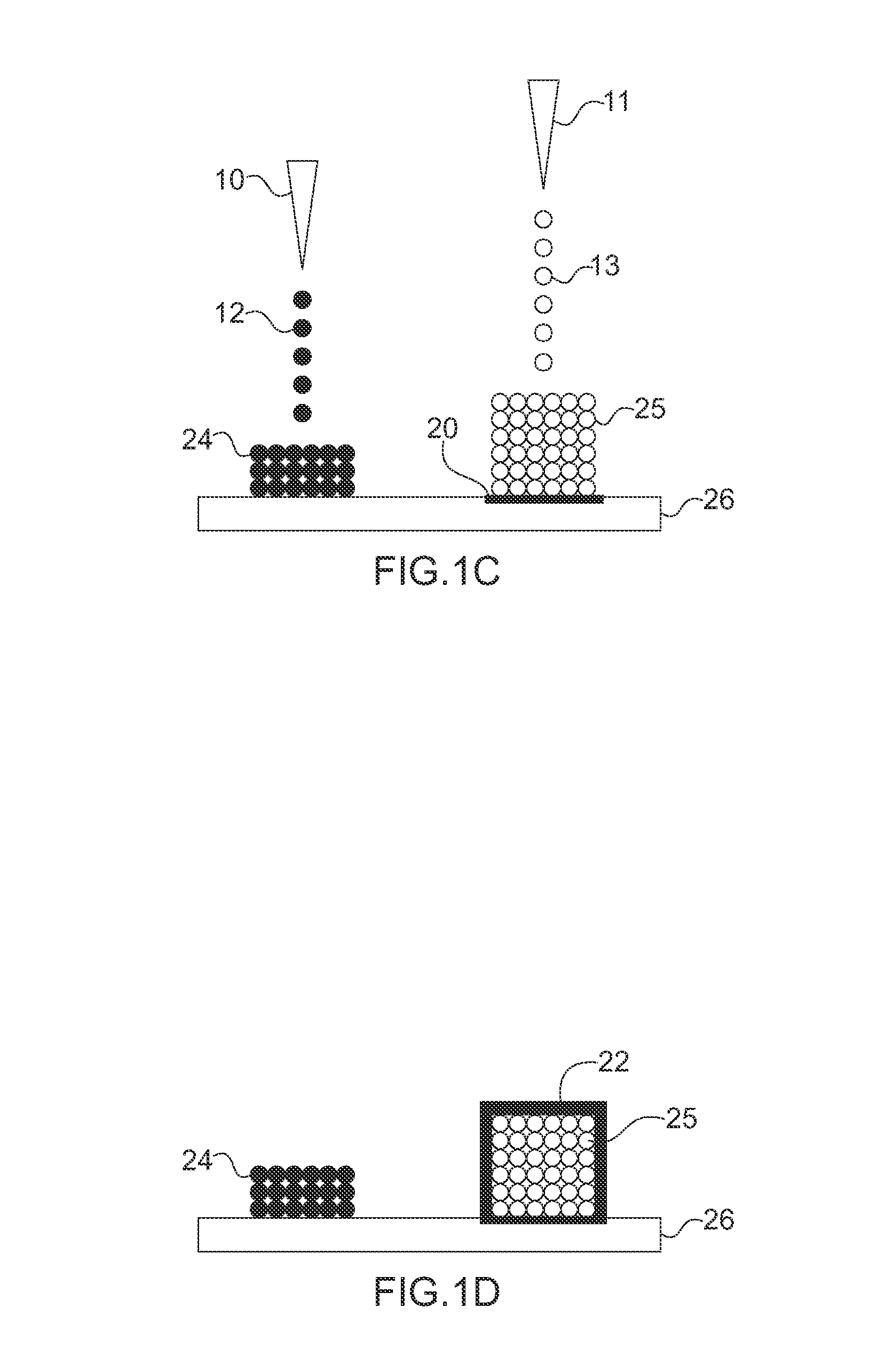
[0030]The present invention relates to processes and devices created, at least in part, utilizing three dimensional (3D) additive build manufacturing as a way to create 3D objects by going from a computer or digital design of the 3D object to the object itself from this digital information. In one of its aspects, the present invention relates to simple and complex electronic and / or mechanical structures and processes for their formation. In one notable aspect, the present invention relates to devices having conductive structures with tolerances and accuracy on the micron scale, such as microwave and waveguide circuits. In this regard, the present invention provides novel methods for creating such conductive structures via 3D additive build manufacturing while overcoming present difficulties in providing conductive structures of small dimension and high tolerance and having suitable bulk electrical and thermal conductivity properties made via 3D additive build manufacturing. In parti...


PUM

PropertyMeasurementUnit
Dielectric polarization enthalpyaaaaaaaaaa
Compositionaaaaaaaaaa
Electrical conductoraaaaaaaaaa

Abstract

The present invention relates to the fabrication of complicated electronic and/or mechanical structures and devices and components using homogeneous or heterogeneous 3D additive build processes. In particular the invention relates to selective metallization processes including electroless and/or electrolytic metallization.

Description

FIELD OF THE INVENTION[0001]The present invention relates to the fabrication of electronic and / or mechanical structures and components and devices such as those used in the electronics industry. In particular, the present invention relates to using homogeneous or heterogeneous materials in three dimensional fabrication of electronic and / or mechanical structures and components and devices. Additionally, the present invention relates to selective metallization processes including electroless and / or electrolytic metallization.BACKGROUND OF THE INVENTION[0002]Improved methods of fabricating electronic and / or mechanical structures continue to drive the electronics and other industries. More and more components are being added to devices that are getting increasingly complex and smaller. As a result fabrication techniques are required to provide electronic and / or mechanical components and / or parts that have increased functionality as well as to take up less space in the device and on subs...

Claims


Application Information

Patent Timeline
IPC IPC(8): B29C70/88B29C67/00C25D5/02B22D19/00
CPCB29C70/882C25D5/02B29C67/0055B22D19/00H05K3/1275H05K3/4664H05K2201/0191H05K2201/0195B29C64/106B33Y80/00H05K1/0284H05K2201/037H05K1/0274H01P11/005H01P3/06B29C67/00
Inventor SHERRER, DAVID W.CARDWELL, DARA L.
Owner CUBIC CORPORATION
Why Eureka
Try Eureka