Sealing structure, device, and method for manufacturing device

a manufacturing device and sealing structure technology, applied in the manufacturing of semiconductor/solid-state devices, semiconductor devices, electrical devices, etc., can solve the problems of heat resistance and color filter damage, and achieve the effect of high reliability and high reliability

Active Publication Date: 2014-09-11
SEMICON ENERGY LAB CO LTD
View PDF5 Cites 144 Cited by
  • Summary
  • Abstract
  • Description
  • Claims
  • Application Information

AI Technical Summary

Benefits of technology

[0013]In view of the above, an object of one embodiment of the present invention is to provide a sealing structure that suppresses heat conduction from a sealant to a sealed component. Another object of one embodiment of the present invention is to provide a sealing structure that suppresses heat conduction from a sealant to a sealed component and allows a device to have a slim bezel. Another object of one embodiment of the present invention is to provide a device in which heat conduction from a sealant to an element with low heat resistant is suppressed. Another object of one embodiment of the present invention is to provide a device in which heat conduction from a sealant to an element with low heat resistant is suppressed and whose bezel is slim. Another object of one embodiment of the present invention is to provide a highly reliable electronic device or a highly reliable lighting device whose bezel is slim.
[0014]Another object of one embodiment of the present invention is to provide a novel sealing structure or a novel device. Another object of one embodiment of the present invention is to provide a highly reliable sealing structure or a highly reliable device. One object of one embodiment of the present invention is to provide a sealing structure that allows a device to have a slim bezel or to provide a device whose bezel is slim.
[0015]Another object of one embodiment of the present invention is to suppress heat damage to a sealed component or a functional element while a sealing structure or a device is manufactured.
[0018]By application of one embodiment of the present invention, heat is not easily conducted from the sealant to the sealed component without increasing the distance between the sealant and the sealed component, and heat damage to the sealed component is thus suppressed. Thus, a surface area of a region where the sealed component can be formed in the substrate can be increased (the bezel of the device can be reduced).
[0030]According to one embodiment of the present invention, a sealing structure in which heat conduction from a sealant to a sealed component is suppressed can be provided. According to one embodiment of the present invention, a sealing structure in which heat conduction from a sealant to a sealed component is suppressed and whose border can be slim can be provided. According to one embodiment of the present invention, a device in which heat conduction from a sealant to a functional element is suppressed can be provided. According to one embodiment of the present invention, a device in which heat conduction from a sealant to a functional element is suppressed and whose border is slim can be provided. According to one embodiment of the present invention, a highly reliable electronic device or a highly reliable lighting device whose border is slim can be provided.

Problems solved by technology

For example, heat resistance of organic EL elements, organic films, or the like is insufficient in many cases, and color filters might be damaged even at approximately 200° C.

Method used


Image

  • Sealing structure, device, and method for manufacturing device
  • Sealing structure, device, and method for manufacturing device
  • Sealing structure, device, and method for manufacturing device

Examples


embodiment 1

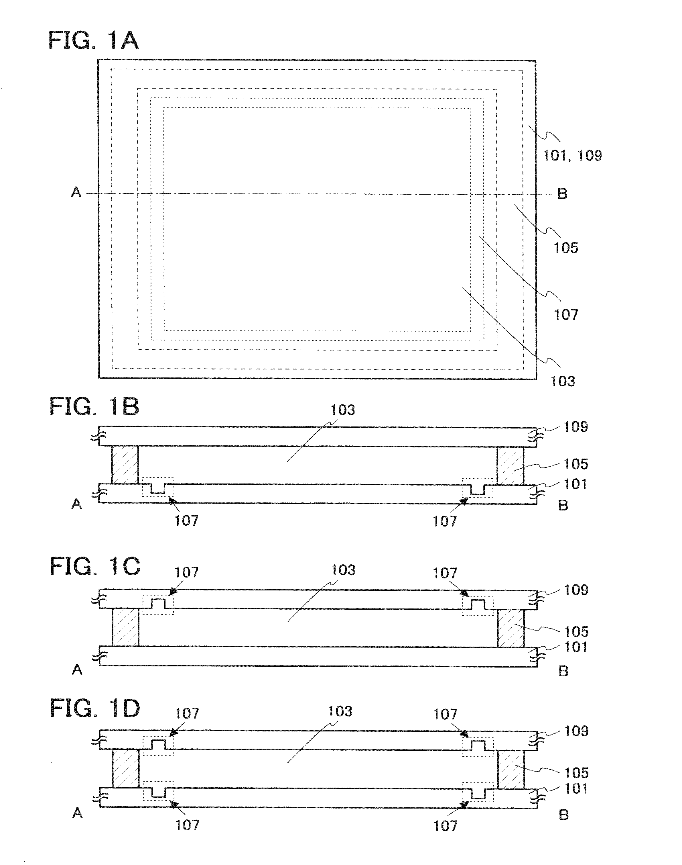
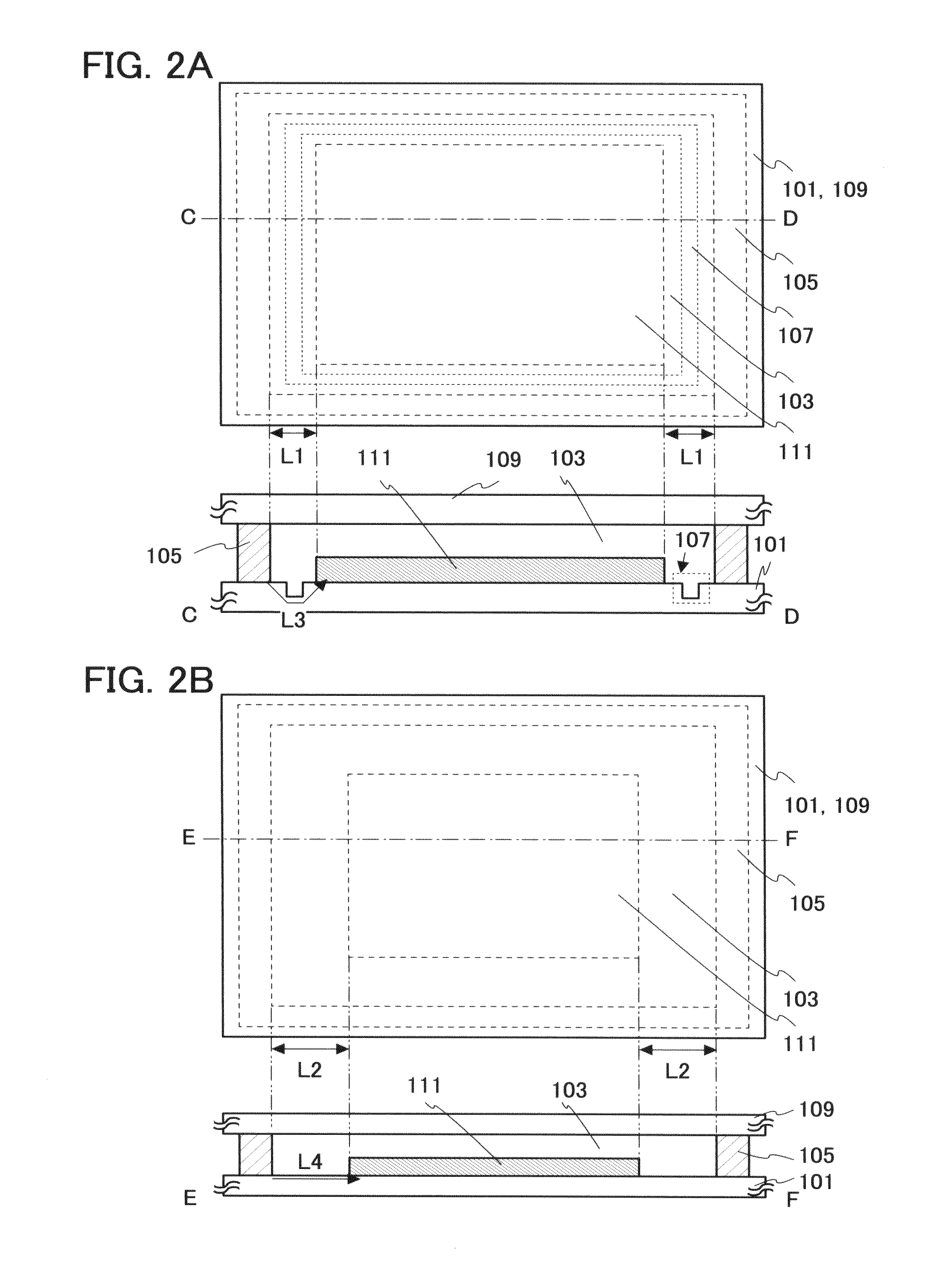
[0052]In this embodiment, a sealing structure of one embodiment of the present invention is described using FIGS. 1A to 1D, FIGS. 2A and 2B, FIGS. 3A to 3E, and FIGS. 4A to 4G.

[0053]FIG. 1A is a plan view of the sealing structure of one embodiment of the present invention. FIGS. 1B to 1D are three kinds of examples of cross-sectional views taken along dashed-dotted line A-B in FIG. 1A.

[0054]As illustrated in FIGS. 1A to 1D, the sealing structure of one embodiment of the present invention includes a substrate 101 and a substrate 109 the first surfaces of which face each other; a frame-like sealant 105 which seals a space 103 with the substrate 101 and the substrate 109; and a groove portion 107 (also referred to as a depressed portion) provided in at least one of the first surface of the substrate 101 and the first surface of the substrate 109. The groove portion 107 is surrounded by the sealant 105.

[0055]The space 103 is in a vacuum or filled with a material having lower heat conduc...

embodiment 2

[0107]In this embodiment, a light-emitting device and a display device which are one embodiment of the present invention are described with reference to FIGS. 5A to 5C, FIGS. 6A to 6C, FIGS. 7A and 7B, and FIGS. 8A and 8B. In this embodiment, a light-emitting device and a display device which include an organic EL element is described as an example.

[0108]FIG. 5A is a plan view of a light-emitting device of one embodiment of the present invention. FIG. 5B is a cross-sectional view taken along dashed-dotted line G-H in FIG. 5A. FIG. 5C is a cross-sectional view taken along dashed-dotted line I-J in FIG. 5A.

[0109]As illustrated in FIGS. 5A to 5C, the light-emitting device of this embodiment of the present invention includes the substrate 101 and the substrate 109 the first surfaces of which face each other; the frame-like sealant 105 which seals the space 103 with the substrate 101 and the substrate 109; and the groove portion 107 and a light-emitting element which are provided in the ...

embodiment 3

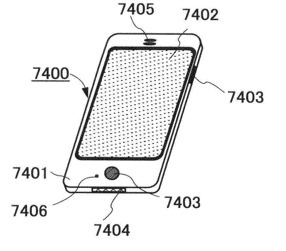
[0146]In this embodiment, examples of electronic devices and lighting devices to which a sealing structure of one embodiment of the present invention is applied will be described with reference to FIGS. 9A to 9E and FIG. 10.

[0147]The electronic devices and lighting devices described in this embodiment have high reliability because an element corresponding to a sealed component (e.g., a semiconductor element, a light-emitting element, or a display element) is sealed in the sealing structure of one embodiment of the present invention.

[0148]Examples of the electronic device using an embodiment of the present invention is applied include: television sets (also called TV or television receivers); monitors for computers or the like; cameras such as digital cameras or digital video cameras; digital photo frames; mobile phones (also called cellular phones or portable telephones); portable game machines; portable information terminals; audio playback devices; and large game machines such as ...


PUM


Abstract

Provided is a device in which heat conduction from a sealant to a functional element is suppressed and whose bezel is slim. The sealing structure includes a first substrate, a second substrate whose surface over which a sealed component is provided faces the first substrate, and a frame-like sealant which seals a space between the first substrate and the second substrate with the first substrate and the second substrate. The second substrate includes a groove portion between the sealant and the sealed component. The groove portion is in a vacuum or includes a substance whose heat conductivity is lower than that of the second substrate.

Description

BACKGROUND OF THE INVENTION[0001]1. Field of the Invention[0002]One embodiment of the present invention relates to a sealing structure in which a pair of substrates are bonded with the use of glass and a method for manufacturing the sealing structure. Another embodiment of the present invention relates to a device including a functional element with low heat resistance and a method for manufacturing the device. Another embodiment of the present invention relates to a semiconductor device, a light-emitting device, and a display device, or a method for manufacturing these devices. For example, one embodiment of the present invention relates to a light-emitting device using an organic electroluminescence (hereinafter also referred to as EL) phenomenon, and a method for manufacturing the light-emitting device.[0003]2. Description of the Related Art[0004]In recent years, development of light-emitting devices and display devices has been actively promoted, and improvements in reliability ...

Claims


Application Information

Patent Timeline
Patent Type & Authority Applications(United States)
IPC IPC(8): H01L33/52H01L33/50
CPCH01L33/507H01L33/52H01L2924/0002H10K59/38H10K59/131H10K50/841H10K50/8426H10K50/87H01L2924/00H10K50/84
Inventor ITO, MINATOYOKOYAMA, KOHEINISHIDO, YUSUKE
Owner SEMICON ENERGY LAB CO LTD
Why Eureka
Try Eureka