
Power Semiconductor Assembly and Module

a technology of power semiconductor and power module, which is applied in the direction of printed circuit manufacturing, printed circuit aspects, manufacturing tools, etc., can solve the problems of increasing the complexity of the fabrication process, the current method of assembling the semiconductor chip package, and the component connected to the semiconductor chip package or the semiconductor chip itsel

Active Publication Date: 2014-09-11
INFINEON TECH AG
View PDF6 Cites 0 Cited by
  • Summary
  • Abstract
  • Description
  • Claims
  • Application Information

AI Technical Summary

Benefits of technology

The present invention provides various devices and methods for assembling power semiconductors. These devices and methods include printed circuit boards, heat sinks, semiconductor chip packages, bumper pads, and pins. These components are used to improve the thermal performance and reliability of power semiconductor assemblies through a variety of techniques such as pressure mounting, heat spreading, and increased contact area. The technical effects of this invention include improved thermal performance, reduced package size, and increased reliability of power semiconductor assemblies.

Problems solved by technology

If the heat sink does not dissipate heat in a desired manner, components connected to the semiconductor chip packages or the semiconductor chip itself may be damaged.
Further, some currently used methods of assembling semiconductor chip packages, such as power modules that reduce heat dissipation, are expensive and may increase the complexity of the fabrication process.

Method used


Image

  • Power Semiconductor Assembly and Module
  • Power Semiconductor Assembly and Module
  • Power Semiconductor Assembly and Module

Examples


Embodiment Construction

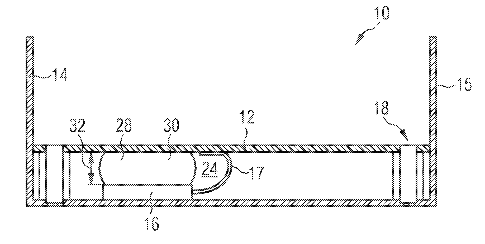
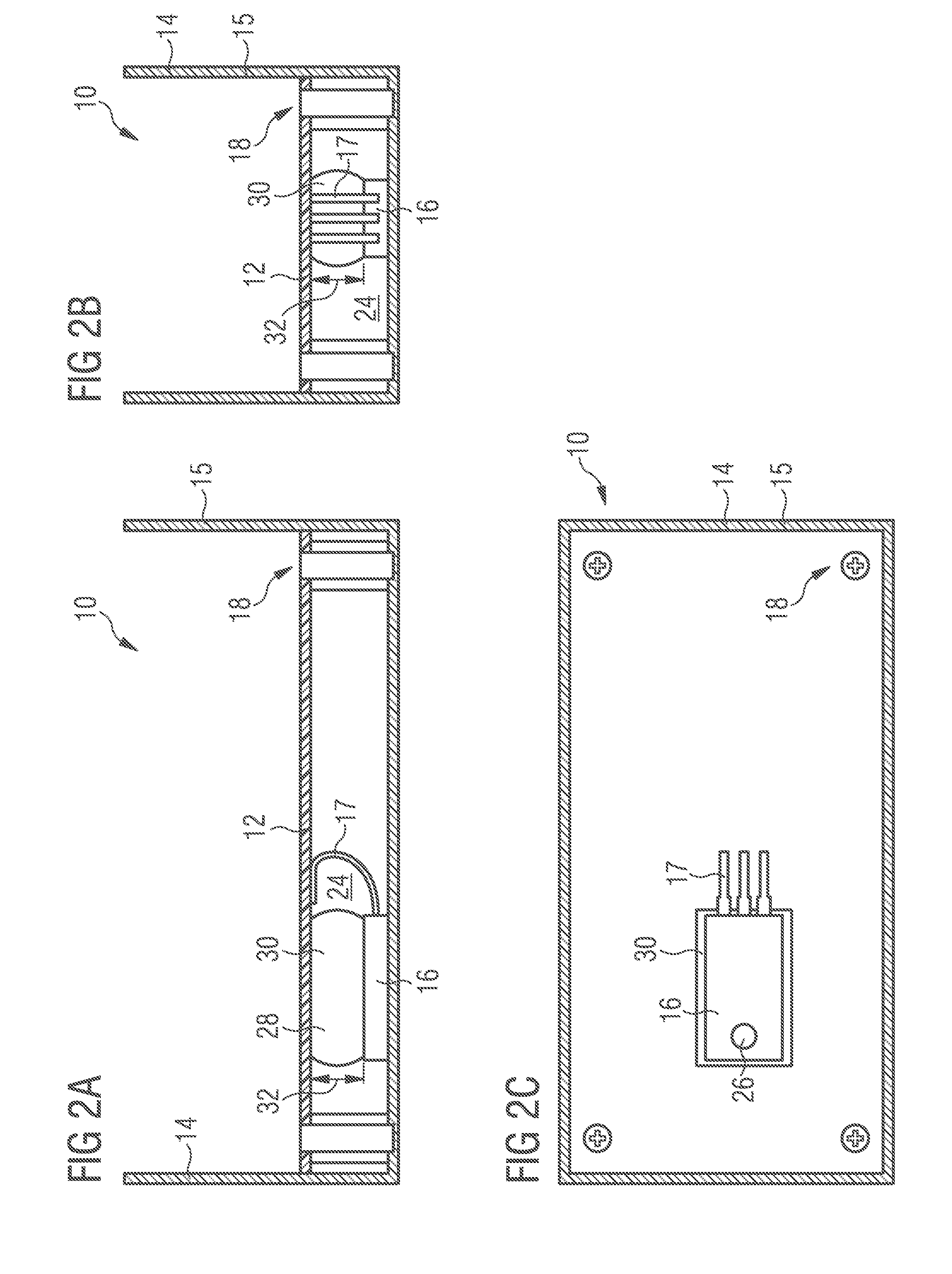
[0032]The making and using of various embodiments are discussed in detail below. It should be appreciated, however, that the present invention provides many applicable inventive concepts that can be embodied in a wide variety of specific contexts. The specific embodiments discussed are merely illustrative of specific ways to make and use the invention and do not limit the scope of the invention.

[0033]In various embodiments, the present invention teaches assembling a semiconductor chip package such that the heat-generating side of the semiconductor chip package is oriented in the direction of a heat sink. Various embodiments use a novel spacing structure to pressure mount the semiconductor chip package to the heat sink thereby obviating the need for screws or other fasteners to connect the semiconductor chip package to the heat sink. In addition, the various embodiments provide the ability to solder the semiconductor chip package to a printed circuit board at the same time as other s...


PUM

PropertyMeasurementUnit
Pressureaaaaaaaaaa
Electrical resistanceaaaaaaaaaa
Flexibilityaaaaaaaaaa

Abstract

A method and apparatus for assembling a power semiconductor is provided. A device includes a printed circuit board, a heat sink, and a semiconductor chip package. The semiconductor chip package is located between the printed circuit board and the heat sink. A heat-generating surface of the semiconductor chip package is oriented such that the heat-generating surface faces the heat sink.

Description

TECHNICAL FIELD[0001]The present invention relates generally to semiconductor devices. In particular, embodiments the present invention relates to a method and apparatus for assembling a power semiconductor device using a spacer.BACKGROUND[0002]In the assembly of semiconductor chip packages, it is desirable to produce the semiconductor chip packages in a way that meets individual needs of consumers. Industrial consumers have a desire to efficiently attach semiconductor packages to boards like printed circuit boards (PCB).[0003]In a semiconductor chip package, the semiconductor chip is embedded or housed within the chip package and the contact pads of the semiconductor chip are connected to external contact elements of the chip package. It is desirable to produce semiconductor chip packages so that their external contact elements allow a higher degree of flexibility with regard to the attachment of the semiconductor chip package to a board. It is also desirable to increase the modula...

Claims


Application Information

Patent Timeline
IPC IPC(8): H01L23/34H01L23/00
CPCH01L24/92H01L23/34H01L23/36H01L23/4006H01L23/42H01L2924/1306H01L2924/13055H01L2924/1305H01L2924/0002H05K1/0203H05K3/3426H05K3/3447H05K2201/10757H05K2201/10765H05K2201/2036H01L2924/00
Inventor CARLETTI, ANDREA
Owner INFINEON TECH AG
Learn More