Semiconductor package including antenna layer and manufacturing method thereof

a technology of semiconductors and semiconductors, applied in the direction of resonant antennas, substantially flat resonant elements, basic electric elements, etc., can solve the problems of reducing the size of the device to achieve compact product design, reducing the quality of the signal transmitted between the antenna and the communication module, and reducing the cost of manufacturing both devices

Active Publication Date: 2014-09-11
ADVANCED SEMICON ENG INC
View PDF6 Cites 60 Cited by
  • Summary
  • Abstract
  • Description
  • Claims
  • Application Information

AI Technical Summary

Problems solved by technology

Accordingly, manufacturing costs are incurred for both devices.
Further, it is difficult to reduce device size to attain compact product design.
In addition, an RF signal transmission path between the antenna and the communication module may be long, reducing the quality of a signal transmitted between the antenna and the communication module.

Method used


Image

  • Semiconductor package including antenna layer and manufacturing method thereof
  • Semiconductor package including antenna layer and manufacturing method thereof
  • Semiconductor package including antenna layer and manufacturing method thereof

Examples


Embodiment Construction

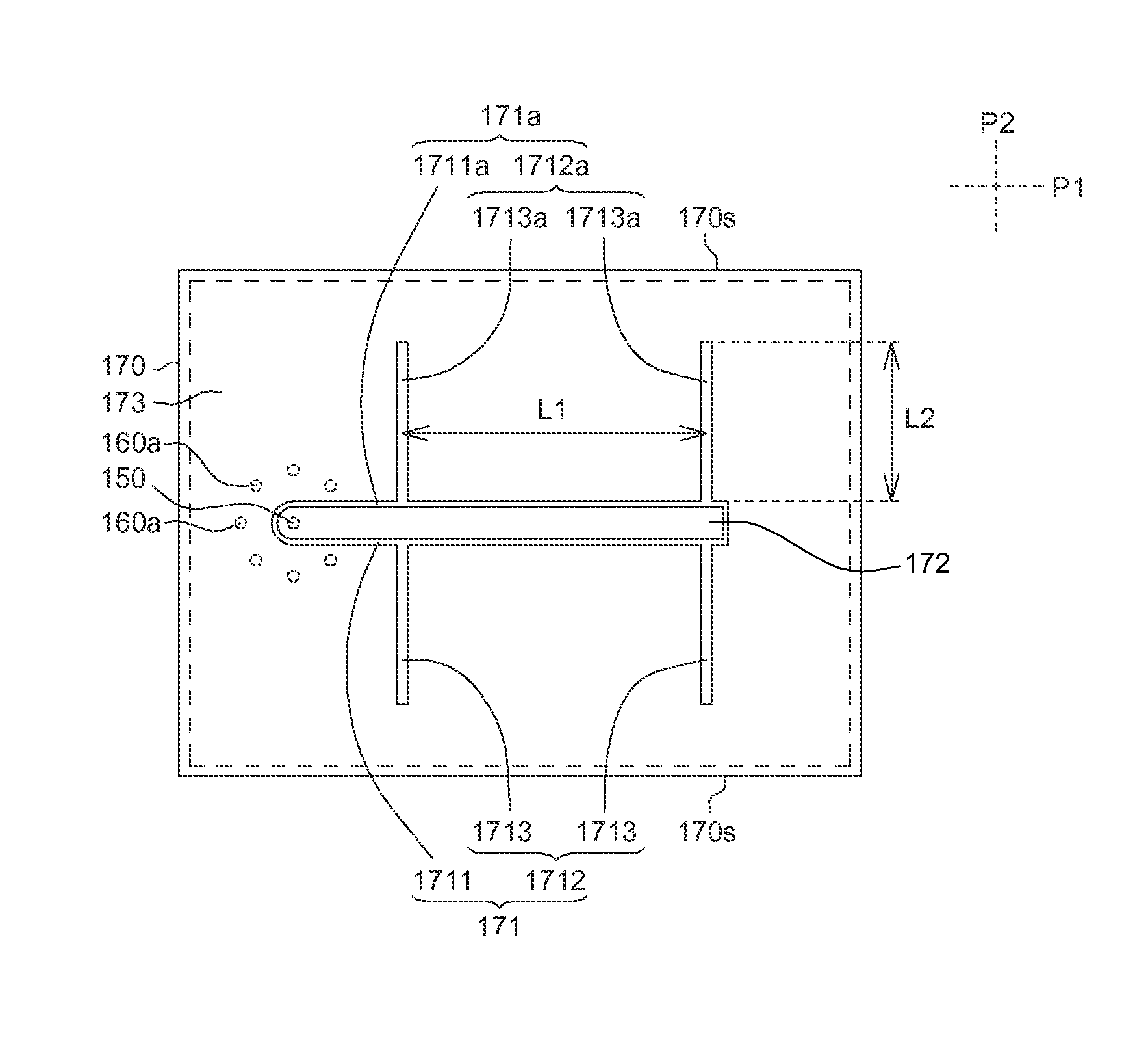
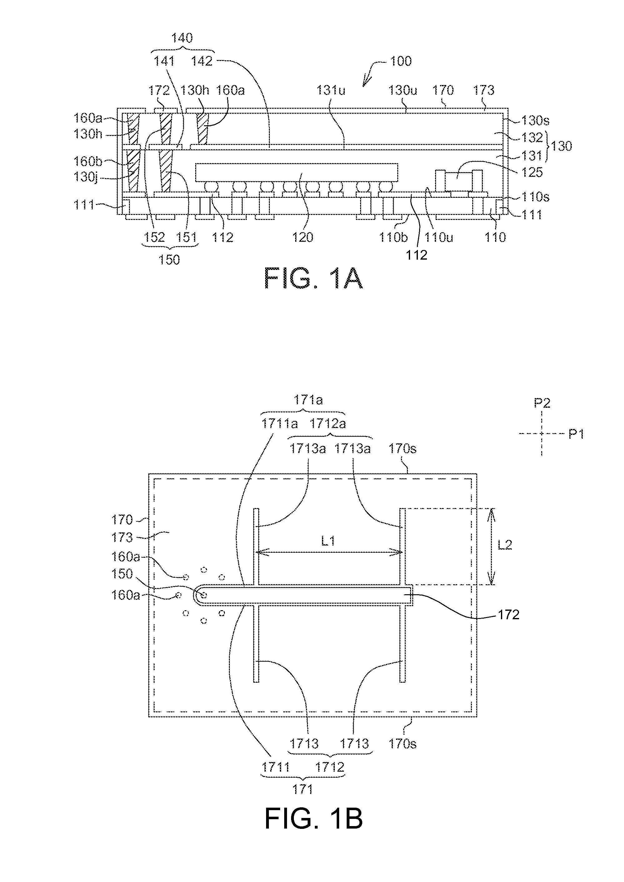
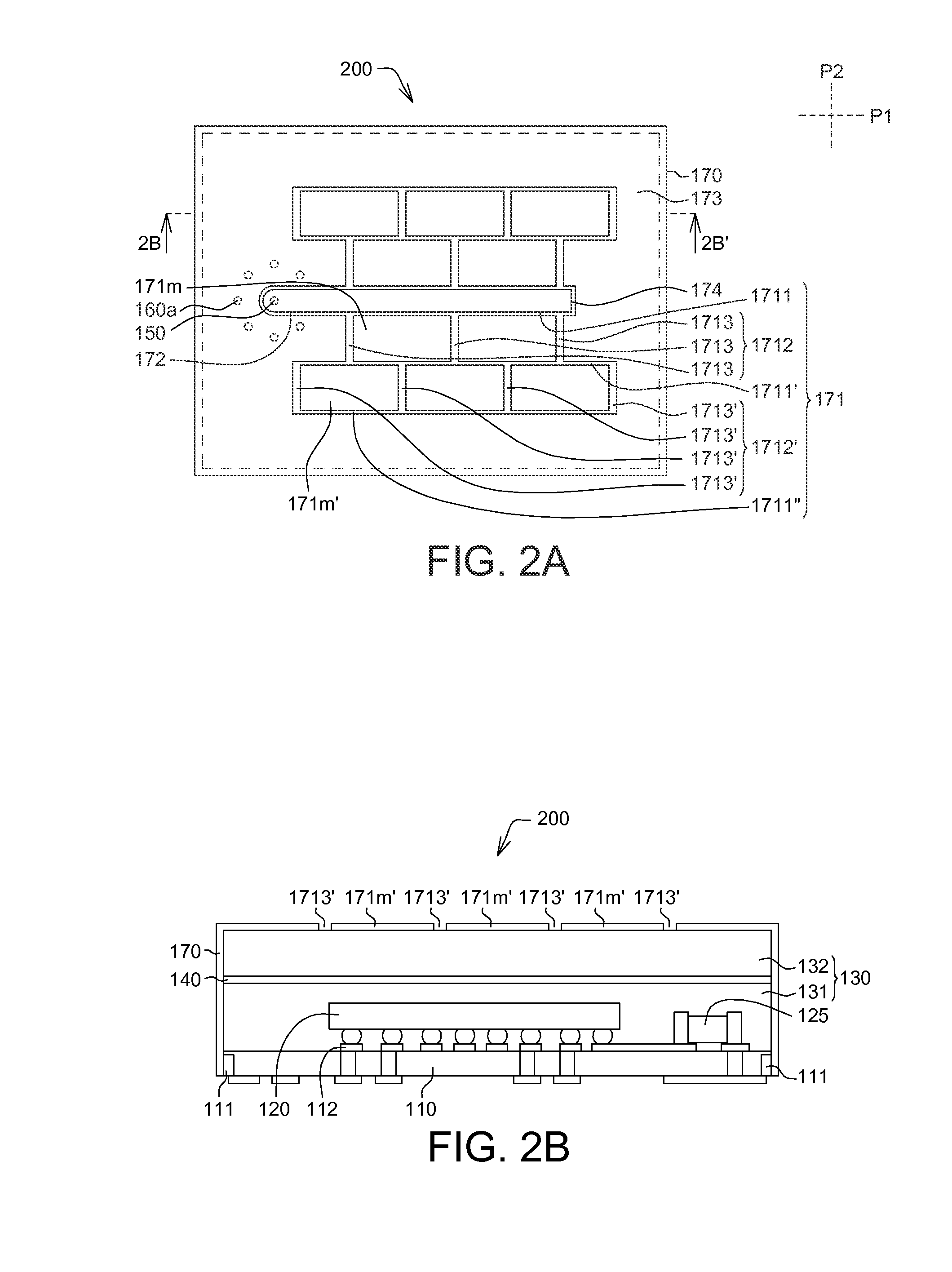
[0025]It is desirable to have the benefits of a single semiconductor package including the antenna portion and the communication module portion of a wireless communication device, such as the benefits of reduced package size and shorter RF signal transmission paths. The embodiments disclosed herein provide such a single semiconductor package.

[0026]Referring to FIG. 1A, a cross-sectional view of an example semiconductor package 100 according to one embodiment is illustrated. The semiconductor package 100 includes a substrate 110, a semiconductor chip 120, a package body 130, a shielding layer 140, a feeding element 150, a plurality of conductive pillars 160 and an antenna layer 170.

[0027]The substrate 110 can be a multi-layered organic substrate or a ceramic substrate, for example. The substrate 110 includes an upper surface 110u, a lower surface 110b opposite to the upper surface 110u and a lateral surface 110s disposed adjacent to a periphery of the substrate 110. The lateral surfa...


PUM


Abstract

A semiconductor package and a manufacturing method thereof are provided. The semiconductor package includes a substrate, a semiconductor chip, a package body and an antenna layer. The semiconductor chip is disposed on the substrate. The package body encapsulates the semiconductor chip and includes an upper surface. The antenna layer is formed on the upper surface of the package body and includes two antenna slot groups connected together. Each antenna slot group includes a wave guiding slot extending along a first direction, and an irradiation slot group extending along a second direction, wherein the irradiation slot group is connected to the wave guiding slot.

Description

BACKGROUND OF THE INVENTION[0001]1. Field of the Invention[0002]The invention relates in general to a semiconductor package and a manufacturing method thereof, and more particularly to a semiconductor package with an antenna layer and a manufacturing method thereof.[0003]2. Description of the Related Art[0004]Wireless communication devices, such as cell phones, typically include antennas for transmitting and receiving radio frequency (RF) signals. Conventionally, a wireless communication device includes therein an antenna and a communication module, each disposed on different parts of a circuit board. Under the conventional approach, the antenna and the communication module are separately manufactured, and electrically connected together after being placed on the circuit board. Accordingly, manufacturing costs are incurred for both devices. Further, it is difficult to reduce device size to attain compact product design. In addition, an RF signal transmission path between the antenna...

Claims


Application Information

Patent Timeline
Patent Type & Authority Applications(United States)
IPC IPC(8): H01L23/498
CPCH01L23/498H01L21/561H01L23/552H01L23/66H01L24/97H01L25/16H01L2223/6677H01L2924/19105H01L2224/16225H01L2224/97H01L2924/15192H01L2924/1531H01L2224/81H01L23/5383H01L23/5389H01L23/49822H01L2924/12042H01L2924/15787H01L2924/00H01L2924/181H01L2924/3025H01L2224/73259H01Q1/2283H01Q9/0407H01Q11/04H01L2924/00012
Inventor YEN, HAN-CHEECHEN, SHIH-YUANLAI, CHIEN-PAICHENG, MING-HSIEN
Owner ADVANCED SEMICON ENG INC
Why Eureka
Try Eureka