High Mobility Transport Layer Structures for Rhombohedral Si/Ge/SiGe Devices

a technology of rhombohedral si/ge/sige and transport layer, which is applied in the direction of thermoelectric device junction materials, semiconductor devices, electrical apparatus, etc., can solve the problems of shortening the life of devices, reducing the mobility of carriers, and requiring extra time and effort for growth of buffer layers, so as to facilitate the growth of rhombohedralally aligned si or sige materials

Active Publication Date: 2014-09-18
NASA +1
View PDF6 Cites 16 Cited by
  • Summary
  • Abstract
  • Description
  • Claims
  • Application Information

AI Technical Summary

Benefits of technology

[0009]Another embodiment is a method of fabricating an electronic device. The method includes providing a trigonal crystal substrate defining a (0001) C-plane. Heat is applied to the substrate to raise the temperature of the substrate to a level that facilitates growth of rhombohedrally aligned Si or SiGe material. A layer of a buffer material selected from the group consisting of group IV semiconductors and alloys formed of group IV semiconductors is grown on the substrate. The layer of buffer material comprises a plurality of rhombohedrally aligned (111)-oriented crystals disposed on the (0001) C-plane of the crystal substrate. A first region of material is grown on the buffer layer. The first region comprises an intrinsic or doped first semiconductor material selected from the group consisting of Si, Ge, SiGe. The first region can comprise a first layer of SiGe, and the method can further include growing a layer of Ge material on the first layer, and growing a second layer of SiGe material on the layer of Ge material, such that the layer of Ge material is disposed between adjacent layers of SiGe material. The first and second layers of SiGe can comprise p±doped SiGe, and the layer of Ge material can comprise p-doped Ge.

Problems solved by technology

However, the atomic lattice constant of Ge is bigger than that of Si, and direct epitaxial growth generates a high density of misfit dislocations which decreases carrier mobility and shortens the life time of devices.
The growth of these buffer layers takes extra time and effort.

Method used


Image

  • High Mobility Transport Layer Structures for Rhombohedral Si/Ge/SiGe Devices
  • High Mobility Transport Layer Structures for Rhombohedral Si/Ge/SiGe Devices
  • High Mobility Transport Layer Structures for Rhombohedral Si/Ge/SiGe Devices

Examples


Embodiment Construction

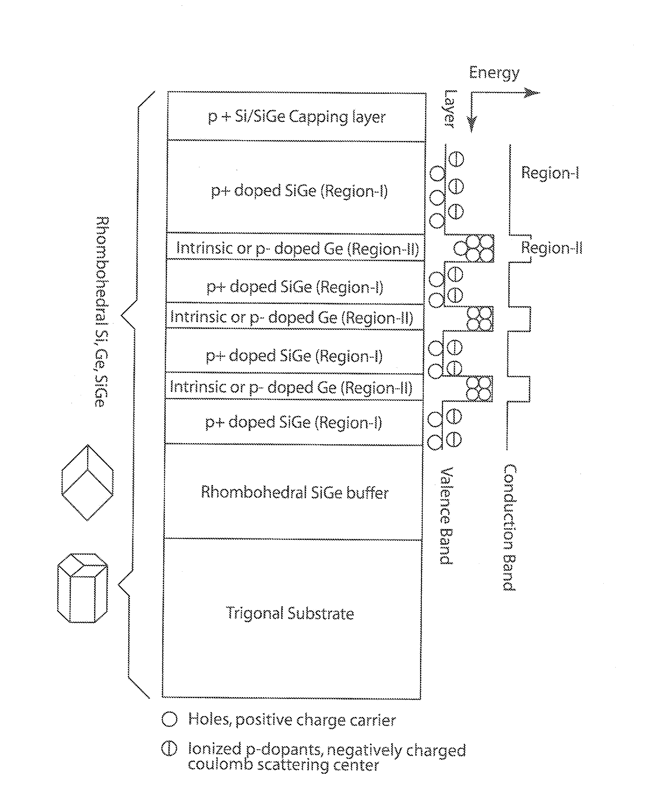
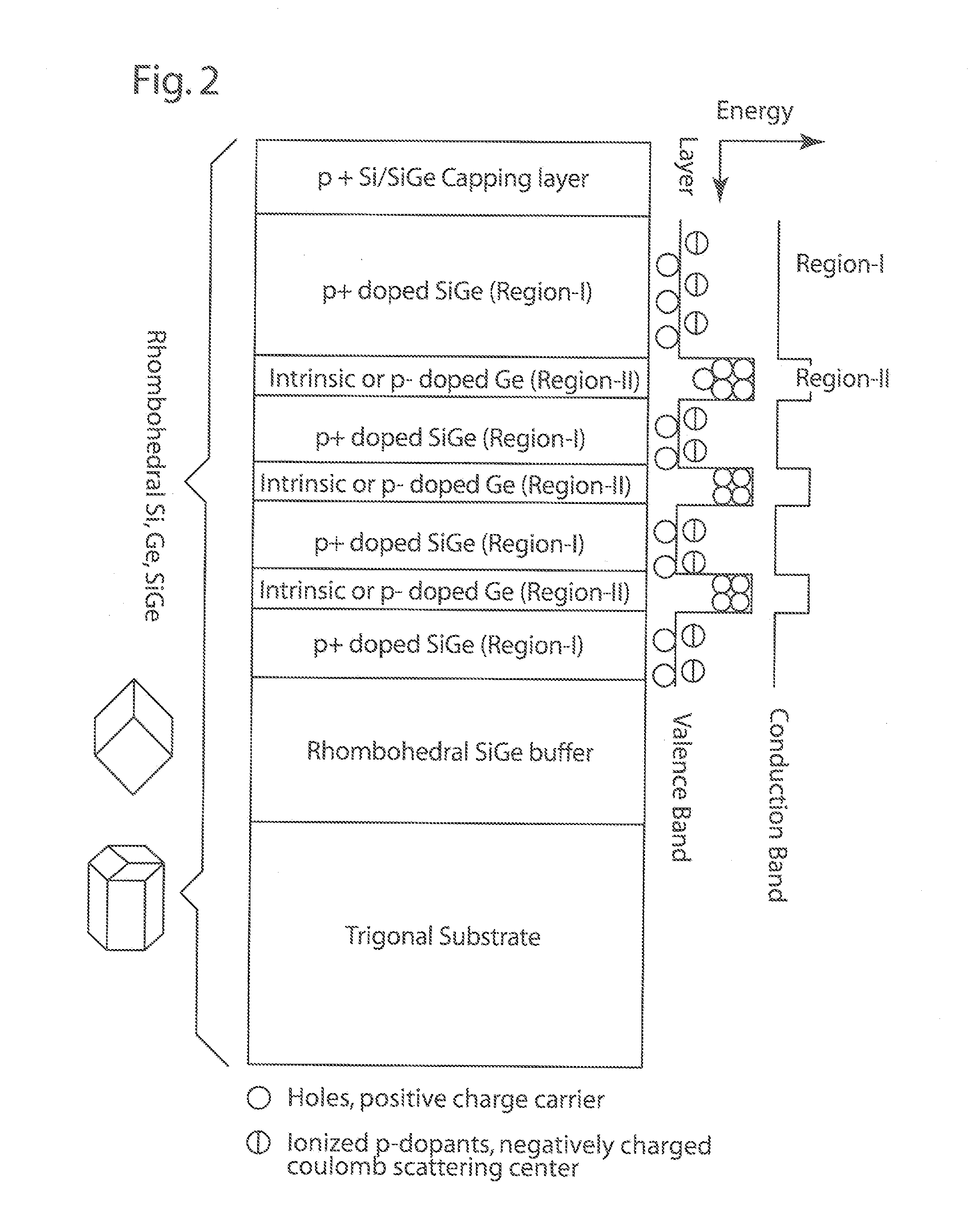
[0019]For purposes of description herein, the terms “upper,”“lower,”“right,”“left,”“rear,”“front,”“vertical,”“horizontal,” and derivatives thereof shall be related to the invention as oriented in FIG. 2. However, it is to be understood that the invention may assume various alternative orientations, except where expressly specified to the contrary. It is also to be understood that the specific devices and processes illustrated in the attached drawings, and as described in the following specification are simply exemplary embodiments of the inventive concepts defined in the appended claims. Furthermore, references to specific items or features shall not be construed as limiting the item or feature to one-piece or multi-piece items or features. Hence, specific dimensions and other physical characteristics relating to the embodiments disclosed herein are not to be considered as limiting, unless the claims expressly state otherwise.

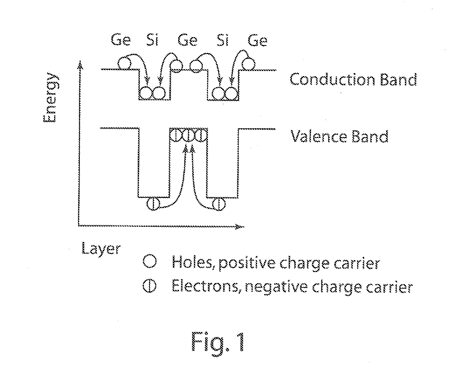
[0020]As discussed above, carrier mobility affects perfor...


PUM


Abstract

An electronic device includes a trigonal crystal substrate defining a (0001) C-plane. The substrate may comprise Sapphire or other suitable material. A plurality of rhomhohedrally aligned SiGe (111)-oriented crystals are disposed on the (0001) C-plane of the crystal substrate. A first region of material is disposed on the rhombohedrally aligned SiGe layer. The first region comprises an intrinsic or doped Si, Ge, or SiGe layer. The first region can be layered between two secondary regions comprising n+doped SiGe or n+doped Ge, whereby the first region collects electrons from the two secondary regions.

Description

CROSS-REFERENCE TO RELATED PATENT APPLICATION(S)[0001]This patent application claims the benefit of and priority to U.S. Provisional Patent Application No. 61 / 779,317, filed on Mar. 13, 2013, the contents of which are hereby incorporated by reference in their entirety.STATEMENT REGARDING FEDERALLY SPONSORED RESEARCH OR DEVELOPMENT[0002]The invention described herein was made in the performance of work under a NASA contract and by employees of the United States Government and is subject to the provisions of Public Law 96-517 (35 U.S.C. §202) and may be manufactured and used by or for the Government for governmental purposes without the payment of any royalties thereon or therefore. In accordance with 35 U.S.C. §202, the contractor elected not to retain title.FIELD OF THE INVENTION[0003]The present invention relates to integrated circuits (“IC”) semiconductor electronic devices, and in particular to an electronic device including a high mobility transport layer such as crystalline SiG...

Claims


Application Information

Patent Timeline
Patent Type & Authority Applications(United States)
IPC IPC(8): H01L29/04H01L29/165H01L21/02
CPCH01L29/045H01L29/165H01L21/02532H01L29/7782H01L29/155H01L31/035236H01L31/03682Y02E10/546H10N10/855H01L21/0242H01L21/02433H01L21/0245H01L21/02516H01L21/02584H01L29/157H01L31/0336
Inventor CHOI, SANG HYOUKPARK, YEONJOONKING, GLEN C.KIM, HYUN-JUNGLEE, KUNIK
Owner NASA
Why Eureka
Try Eureka