
Display control circuit, electro-optical device and electronic apparatus

a control circuit and electronic equipment technology, applied in the field of display control circuits, can solve the problems of degrading display image quality and reducing display quality, and achieve the effect of suppressing vertical crosstalk and minimizing display quality

Inactive Publication Date: 2014-09-18
SEIKO EPSON CORP
View PDF6 Cites 10 Cited by
  • Summary
  • Abstract
  • Description
  • Claims
  • Application Information

AI Technical Summary

Benefits of technology

The invention minimizes the impact on display quality and reduces vertical crosstalk when showing different images. By updating correction data and analyzing the movement of objects, the invention reduces the possibility of rapid display gradation changes when performing vertical crosstalk correction, resulting in a high display quality even for moving images.

Problems solved by technology

As a result, a quality of a display image is degraded.
Then, as the result of the change of such display gradation being visually recognized, there is a problem that a display quality is decreased.

Method used


Image

  • Display control circuit, electro-optical device and electronic apparatus
  • Display control circuit, electro-optical device and electronic apparatus
  • Display control circuit, electro-optical device and electronic apparatus

Examples


first embodiment

A. First Embodiment

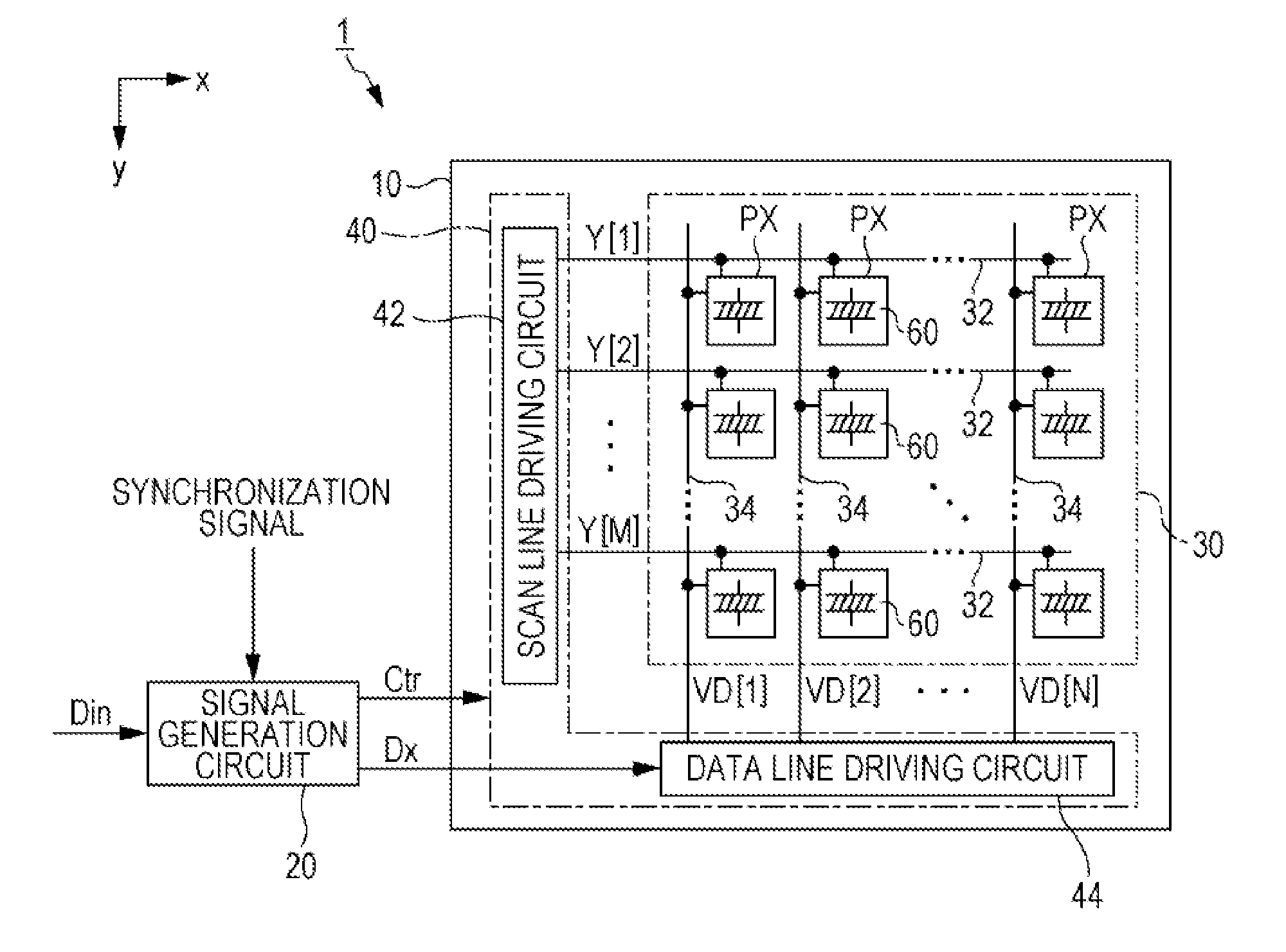
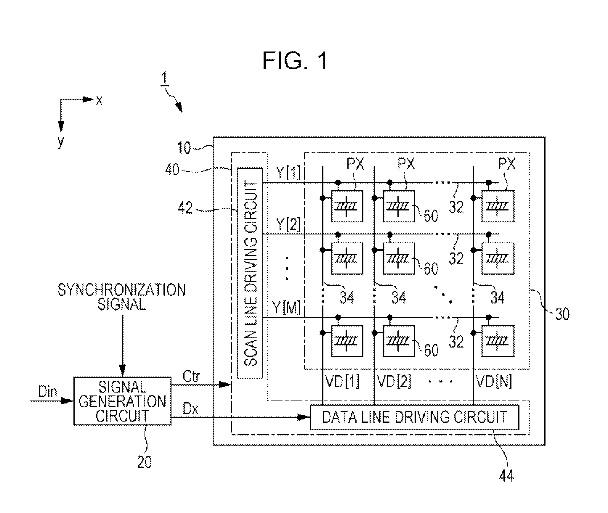
[0053]FIG. 1 is a block diagram of an electro-optical device 1 according to a first embodiment of the present invention.

[0054]The electro-optical device 1 includes an electro-optical panel 10 and a signal generation circuit 20. The electro-optical panel 10 includes a display unit 30 in which a plurality of pixel circuits PX are arranged, and a driving circuit 40 which drives each pixel circuit PX.

[0055]In the display unit 30, M scan lines 32 extending in the x direction and N data lines 34 which extends in the y direction and intersects the x direction, are formed (M and N are natural numbers). The plurality of pixel circuits PX are arranged in a matrix with M vertical rows×N horizontal columns in the display unit 30 corresponding to each intersection of the scan line 32 and the data line 34. In addition, in the present embodiment, the pixel circuits PX are all arranged at the intersections of M×N numbers formed by the M scan lines 32 and the N data lines 34, but ...

second embodiment

B. Second Embodiment

[0204]In the first embodiment, the predetermined number Z which is the number of pixel circuits PX configuring the target pixel circuit, the value W1 which is the number of pixel circuits PX configuring the left target pixel circuits PXL, and the value W2 which is the number of pixel circuits PX configuring the right target pixel circuits PXR are values determined in advance.

[0205]Whereas, the electro-optical device according to the second embodiment is different from the electro-optical device 1 according to the first embodiment, in a point where the predetermined number Z, the value W1 and the value W2 are determined based on the amount of movement Mv in the extending direction of the scan line 32 of the object denoted by the image displayed in the display unit. Hereinafter, the electro-optical device according to the second embodiment will be described with reference to FIGS. 13 and 14A to 14D.

[0206]The electro-optical device according to the second embodiment...

modification example

C. Modification Example

[0222]Each of the above-described forms can be modified in various ways. Aspects of specific modification will be exemplified below. Aspects, which are arbitrarily selected from the following examples, equal to or more than two can be appropriately combined to the extent not inconsistent with each other.


PUM


Abstract

A signal generation circuit of an electro-optical device includes a generation unit that generates correction data corresponding to each pixel circuit based on input image data, a specification unit that, when a value which denotes a difference of two pieces of correction data corresponding to two pixel circuits adjacent to each other is equal to or greater than a predetermined threshold, specifies the two pixel circuits as boundary pixel circuits, an updating unit that generates updated correction data by modifying each value of a predetermined number of pieces of correction data corresponding to a predetermined number of pixel circuits including at least one of the boundary pixel circuits so as to be a value between two values indicated by the two pieces of correction data corresponding to the boundary pixel circuits.

Description

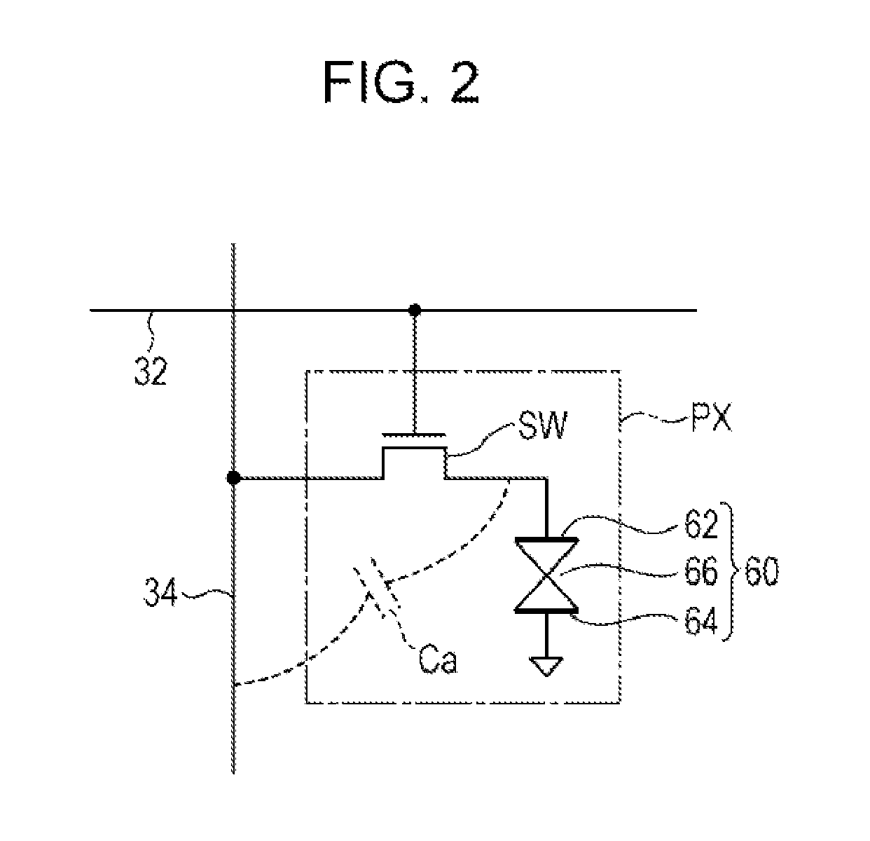
BACKGROUND[0001]1. Technical Field[0002]The present invention relates to a display control circuit, an electro-optical device and an electronic apparatus.[0003]2. Related Art[0004]A liquid crystal display device is known as an example of an electro-optical device that includes an electro-optical element in which an optical characteristic is changed by electric energy. The liquid crystal display device includes a plurality of data lines and a plurality of scan lines, and includes a plurality of pixel circuits each of which is installed in an intersection between the data line and the scan line. The pixel circuit includes a selection transistor, an electro-optical element such as a liquid crystal element. An ON state or an OFF state of the selection transistor is controlled in response to a scan signal supplied through the scan line. When the selection transistor is in the ON state, an image signal supplied through the data line is applied to the liquid crystal element, and when the s...

Claims


Application Information

Patent Timeline
Patent Type & Authority Applications(United States)
IPC IPC(8): G09G3/36
CPCG09G3/3607G09G3/3614G09G3/3648G09G3/3688G09G2320/0214G09G2320/0219
Inventor WAKABAYASHI, JUNICHIHOSAKA, HIROYUKIICHIMURA, HIROAKI
Owner SEIKO EPSON CORP
Learn More