Winding-type solid electrolytic capacitor package structure without using a lead frame and method of manufacturing the same
- Summary
- Abstract
- Description
- Claims
- Application Information
AI Technical Summary
Benefits of technology
Problems solved by technology
Method used
Image
Examples
first embodiment
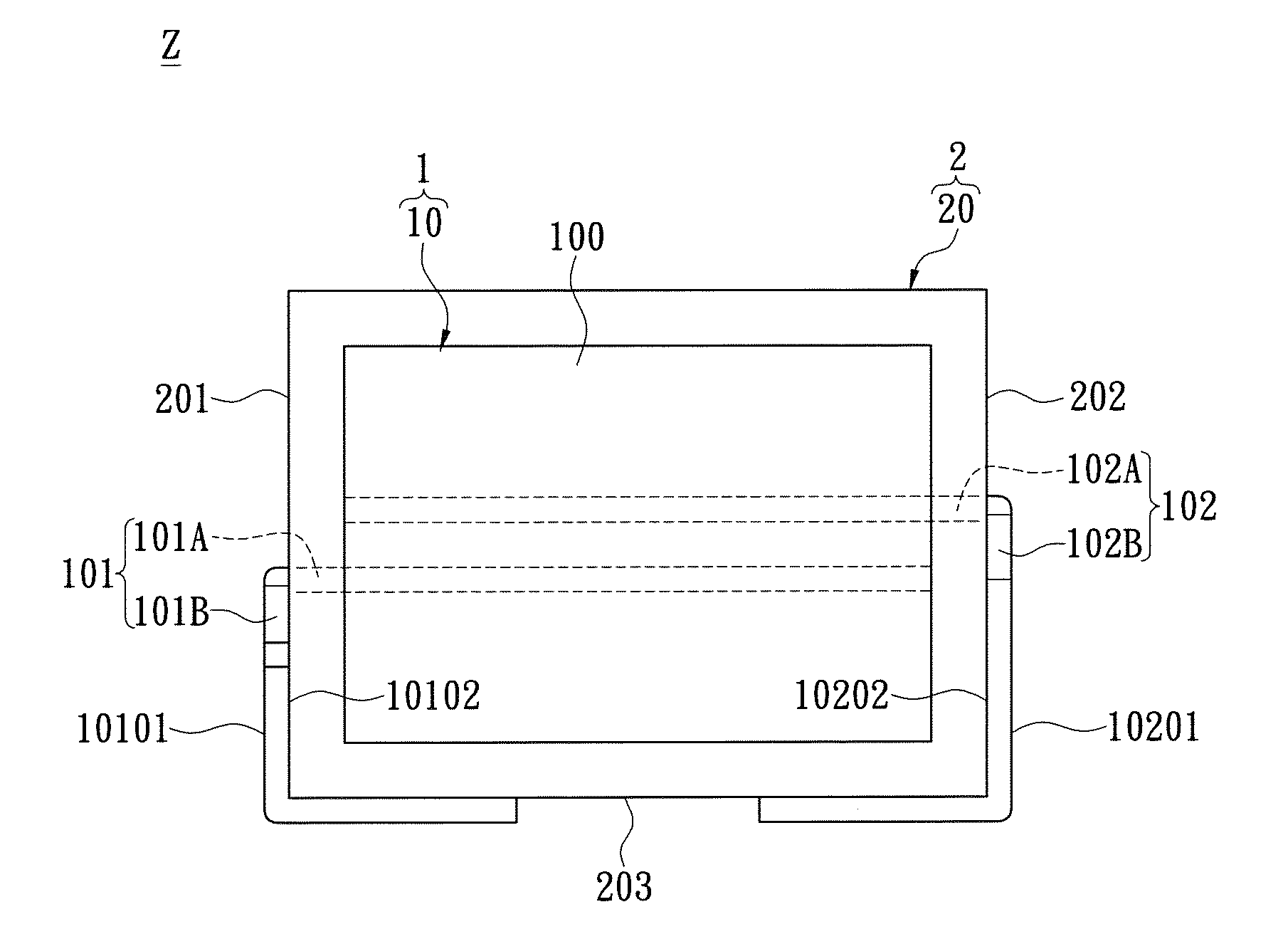
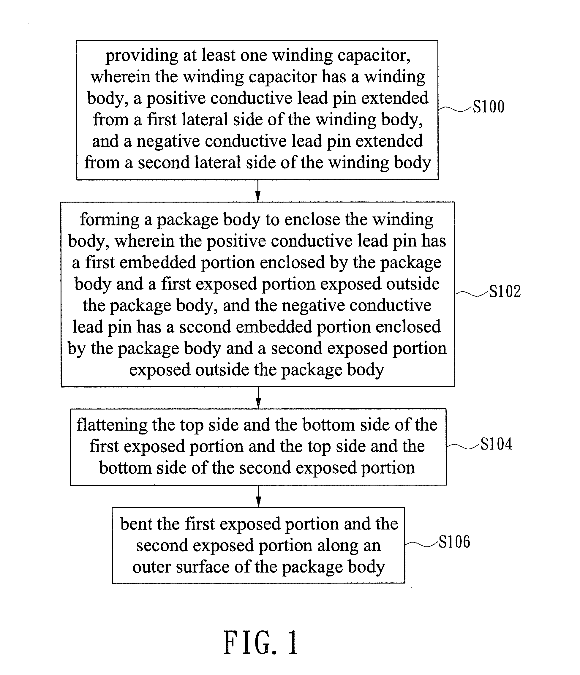
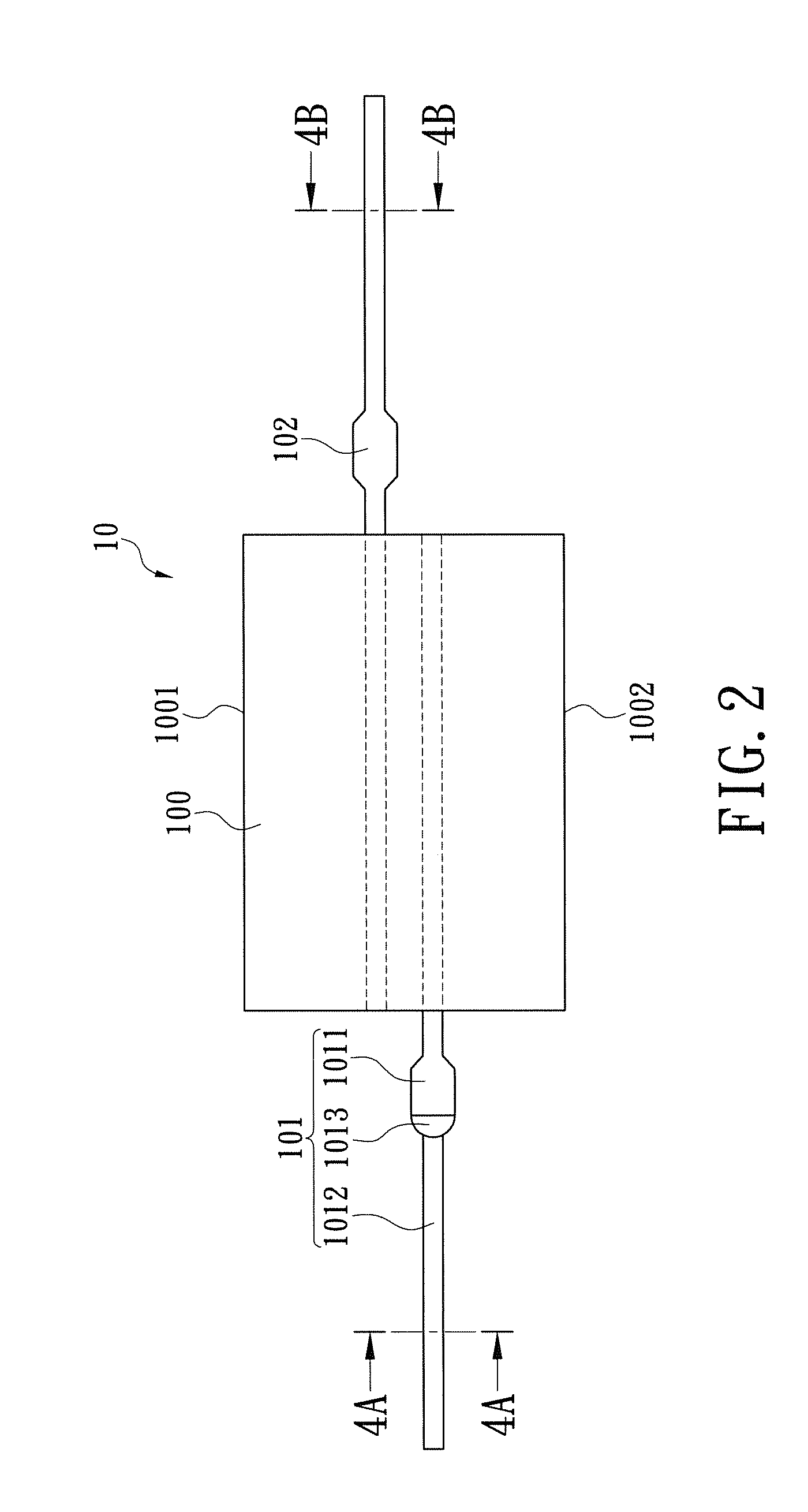
[0030]Referring to FIG. 1 to FIG. 7, where FIG. 1 shows a flowchart of the method of manufacturing a winding-type solid electrolytic capacitor package structure, FIG. 2 shows a front, schematic view of both the first exposed portion and the second exposed portion having not been flattened yet, FIG. 3 shows a perspective, schematic view of the winding body, FIG. 4A shows a cross-sectional view taken along the section line 4A-4A of FIG. 2, FIG. 4B shows a cross-sectional view taken along the section line 4B-4B of FIG. 2, FIG. 5 shows a front, schematic view of the winding body having been enclosed by the package body, FIG. 6 shows a front, schematic view of both the first exposed portion and the second exposed portion having been flattened, and FIG. 7 shows a front, schematic view of both the positive conductive lead pin and the negative conductive lead pin having been bent according to the first embodiment of the instant disclosure. The first embodiment of the instant disclosure prov...
second embodiment
[0039]Referring to FIG. 8 to FIG. 10, where FIG. 9 shows a cross-sectional view taken along the section line A-A and B-B of FIG. 8, and the second embodiment of the instant disclosure provides a winding-type solid electrolytic capacitor package structure Z without using any lead frame comprising: a capacitor unit 1 and a package unit 2. Comparing FIG. 8 with FIG. 2 and comparing FIG. 9 with FIG. 4A and FIG. 4B the difference between the second embodiment and the first embodiment is as follows: in the second embodiment, both the positive conductive lead pin 101 and the negative conductive lead pin 102 can be formed as one-piece structures without using a precision soldering process, thus there is no any soldering point on the positive conductive lead pin 101 and the negative conductive lead pin 102 for decreasing the impedance and the length of the conductive lead pin and increasing the current carrying capacity. In addition, the positive conductive lead pin 101 may be a first multil...
third embodiment
[0041]Referring to FIG. 11 to FIG. 13, where FIG. 12 shows a cross-sectional view taken along the section line A-A and B-B of FIG. 11, and the third embodiment of the instant disclosure provides a winding-type solid electrolytic capacitor package structure Z without using any lead frame comprising: a capacitor unit 1 and a package unit 2. Comparing FIG. 11 with FIG. 8 and comparing FIG. 12 with FIG. 9, the difference between the third embodiment and the second embodiment is as follows: in the third embodiment, the positive conductive lead pin 101 has a first positive conductive portion 1011 electrically contacting the positive foil sheet 100A, a second positive conductive portion 1012, and a first soldering portion 1013 connected between the first positive conductive portion 1011 and the second positive conductive portion 1012. And, the negative conductive lead pin 102 has a first negative conductive portion 1021 electrically contacting the negative foil sheet 100B, a second negativ...
PUM
| Property | Measurement | Unit |
|---|---|---|
| Electrical conductor | aaaaa | aaaaa |
Abstract
Description
Claims
Application Information


