Methods for forming silicon nitride thin films

Active Publication Date: 2014-09-18
ASM IP HLDG BV
View PDF8 Cites 82 Cited by
  • Summary
  • Abstract
  • Description
  • Claims
  • Application Information

AI Technical Summary

Problems solved by technology

However, PEALD using HCDS does not exhibit opt

Method used


Image

  • Methods for forming silicon nitride thin films
  • Methods for forming silicon nitride thin films
  • Methods for forming silicon nitride thin films

Examples


Example

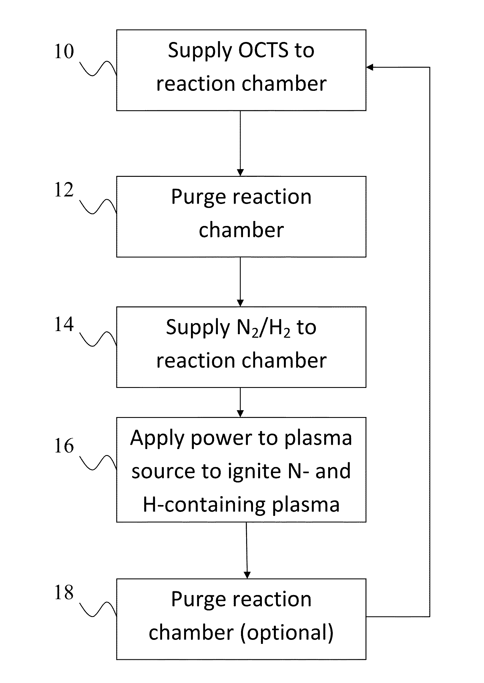
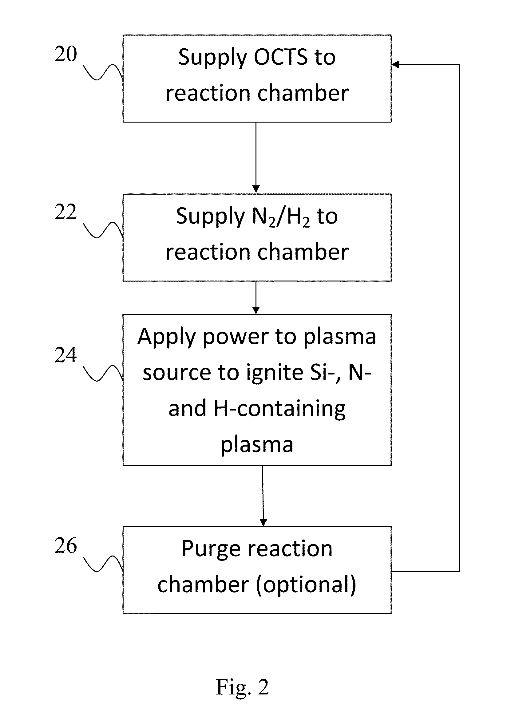
[0020]Silicon nitride has a wide variety of applications, as will be apparent to the skilled artisan. Silicon nitride thin films can be deposited on a substrate by plasma-enhanced atomic layer deposition (PEALD)-type processes. The thickness and composition of each of the layers can be controlled to produce a SiNx film with the desired characteristics.

[0021]ALD type processes are based on controlled, self-limiting surface reactions of precursor chemicals. Gas phase reactions are avoided by contacting the substrate alternately and sequentially with the precursors. Vapor phase reactants are separated from each other in the reaction chamber, for example, by removing excess reactants and / or reactant byproducts from the reaction chamber between reactant pulses.

[0022]The methods presented herein allow deposition of silicon nitride films on substrate surfaces. Geometrically challenging applications are also possible due to the nature of the ALD-type processes. According to some embodiments...


PUM

PropertyMeasurementUnit
Temperatureaaaaaaaaaa

Abstract

The present invention relates to methods of forming silicon nitride thin films on a substrate in a reaction chamber by plasma enhanced atomic layer deposition (PEALD). Exemplary methods include the steps of (i) introducing an octahalotrisilane Si3X8 silicon precursor, such as octachlorotrisilane (OCTS) Si3Cl8, into a reaction space containing a substrate, (ii) introducing a nitrogen containing plasma into the reaction space, and wherein steps (i), (ii) and any steps in between constitute one cycle, and repeating said cycles a plurality of times until an atomic layer nitride film having a desired thickness is obtained.

Description

FIELD OF THE INVENTION[0001]The present application relates generally to atomic layer deposition of silicon nitride thin films.BACKGROUND OF THE INVENTION[0002]With the scaling down of devices, deposition of dielectric films having good step coverage is desirable. Traditional ALD is a self-limiting process, whereby alternated pulses of reaction precursors saturate a substrate surface and leave no more than one monolayer of material per pulse. The deposition conditions and precursors are selected to ensure self-saturating reactions, such that an adsorbed layer in one pulse leaves a surface termination that is non-reactive with the additional gas phase reactants of the same pulse. A subsequent pulse of different reactants reacts with the previous termination to enable continued deposition. Thus each cycle of alternated pulses leaves no more than about one molecular layer of the desired material. The principles of ALD type processes have been presented by T. Suntola, e.g. in the Handbo...

Claims


Application Information

Patent Timeline
IPC IPC(8): H01L21/02
CPCH01L21/0228H01L21/0217C23C16/345C23C16/4554C23C16/45553H01L21/02211H01L21/02274
Inventor NISKANEN, ANTTIHAUKKA, SUVIANTTILA, JAAKKO
Owner ASM IP HLDG BV
Why Eureka
Try Eureka