Casing of electronic device and method of manufacturing the same

a technology of electronic devices and casings, which is applied in the direction of casings/cabinets/drawers, electrical apparatus casings/cabinets/drawers, instruments, etc., can solve the problems of uneven dyeing in the subsequent dyeing process, affecting the quality of the exterior casing of the electronic device, and affecting the color exterior

Active Publication Date: 2014-09-25
HTC CORP
View PDF9 Cites 144 Cited by
  • Summary
  • Abstract
  • Description
  • Claims
  • Application Information

AI Technical Summary

Benefits of technology

[0005]The invention is directed to a method of manufacturing a casing of an electronic device, capable of preventing a process solvent from remaining on surfaces of the casing, so as to solve uneven dyeing of the casing of the electronic device.

Problems solved by technology

The metal parts and the plastic parts may be bonded by adhesives, but such method may lead to steps or gaps generated by differences in element sizes or assembly tolerances between the metal parts and the plastic parts, which affects quality of the casing of the electronic device in terms of exterior.
During manufacturing processes, if the metal parts of the casing of the electronic device are dyed before bonding the metal parts and the plastic parts, the metal parts are prone to damages from molds in the insert molding process or the in-mold process, which affects the color exterior.
If the metal parts and the plastic parts are bonded before dyeing the casing of the electronic device by the anodizing process, an airtight ability between the metal parts and the plastic parts may be insufficient, such that a process solvent used in the anodizing process may easily be remained in between the two, resulting a problem of uneven dyeing in the subsequent dyeing process.

Method used


Image

  • Casing of electronic device and method of manufacturing the same
  • Casing of electronic device and method of manufacturing the same
  • Casing of electronic device and method of manufacturing the same

Examples


Embodiment Construction

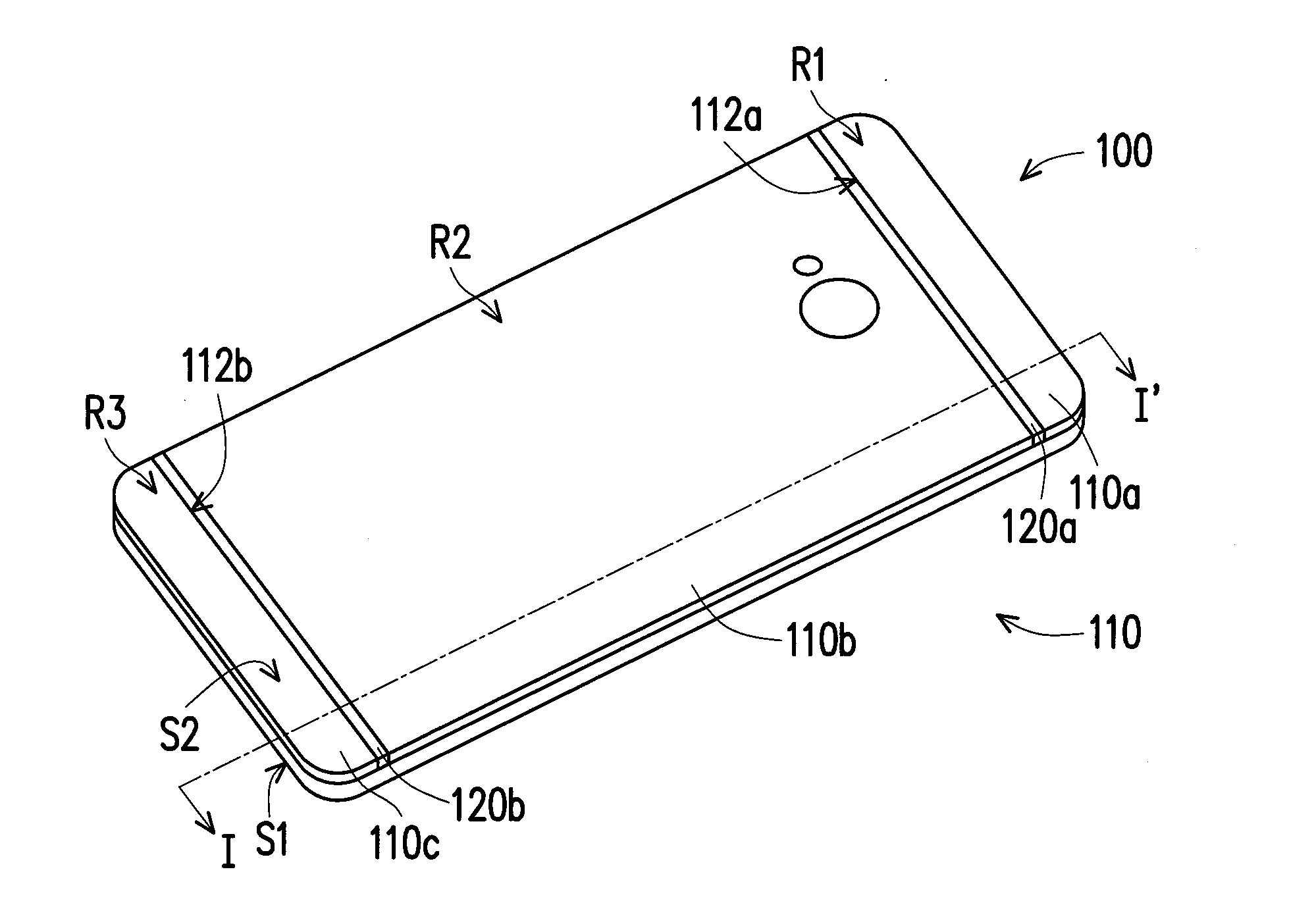
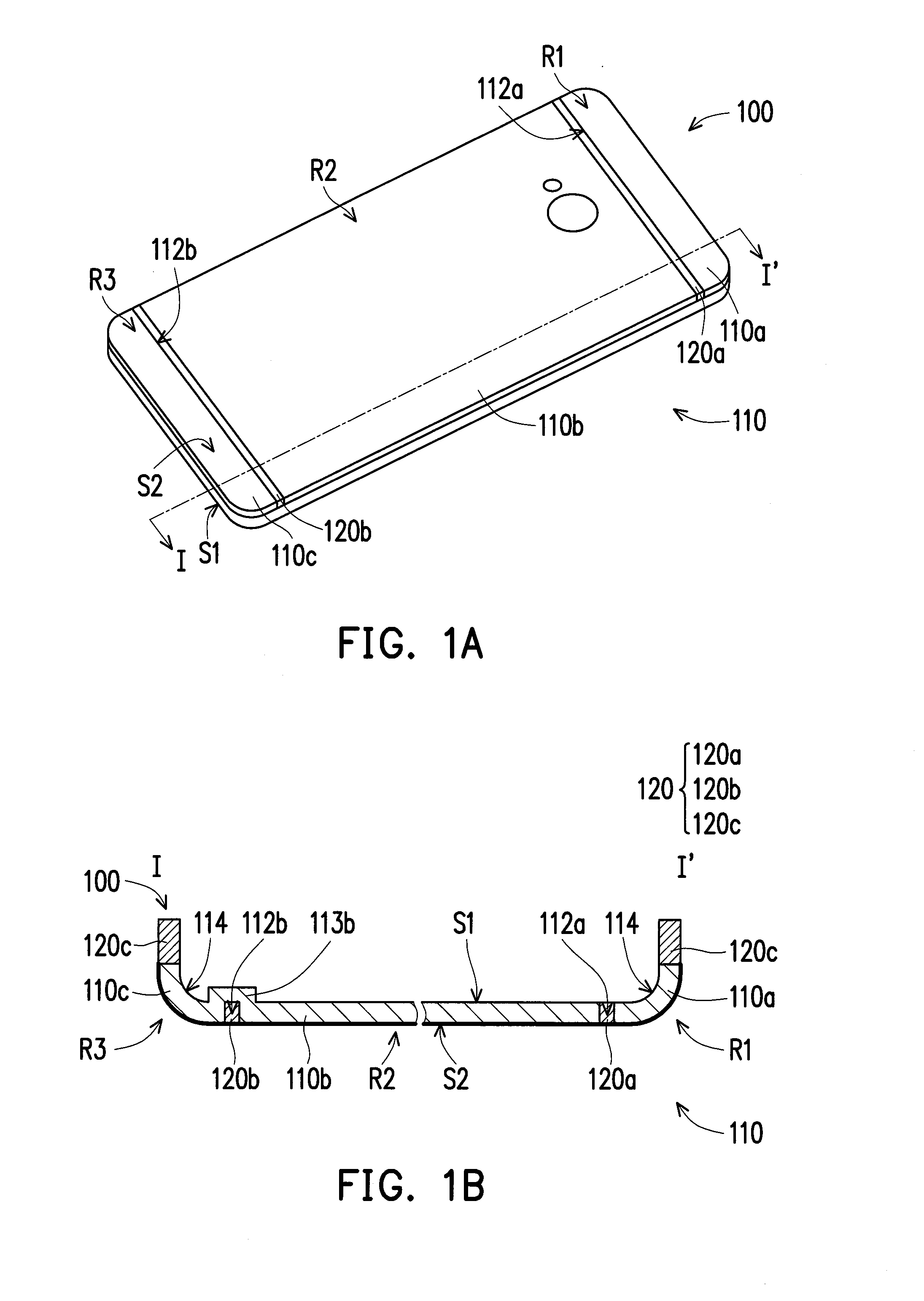
[0018]FIG. 1A is a schematic diagram of a casing of an electronic device according to an embodiment of the invention. FIG. 1B is a cross-sectional diagram of the electronic device of FIG. 1A taken along line I-I′. Referring to FIG. 1A and FIG. 1B, in the present embodiment, a casing 100 of an electronic device includes a metallic housing 110, a first non-conductive spacer 120a and a second non-conductive spacer 120b, wherein the metallic housing 110 includes an inner surface S1 and an outer surface S2 opposite to the inner surface S1. The inner surface S1 is recessed inwardly to substantially form a recessed structure, so that the rest of components (e.g., a battery, a circuit board or an audio device) of an electronic device (not illustrated) may be disposed in the casing 100 of the electronic device. The casing 100 of the electronic device may be used to cover the rest of components suitable for the electronic device, so as to form the electronic device. The electronic device is, ...


PUM

PropertyMeasurementUnit
inner diameteraaaaaaaaaa
non-conductiveaaaaaaaaaa
metallicaaaaaaaaaa

Abstract

A method of manufacturing a casing of an electronic device including the following steps is provided. A metallic housing is provided, wherein the metallic housing has an inner surface and an outer surface opposite to the inner surface. A plurality of apertures are formed on the inner surface of the metallic housing. A non-conductive layer is formed on the inner surface of the metallic housing, and part of the non-conductive layer is extended into the apertures. The outer surface of the metallic housing is dyed to form the casing of the electronic device. A casing of an electronic device is also provided.

Description

CROSS-REFERENCE TO RELATED APPLICATION[0001]This application claims the priority benefits of U.S. provisional application Ser. No. 61 / 804,160, filed on Mar. 21, 2013. The entirety of the above-mentioned patent application is hereby incorporated by reference herein and made a part of this specification.TECHNICAL FIELD[0002]The invention relates to a casing and a manufacturing method, and particularly to a casing of an electronic device and a method of manufacturing the same.RELATED ART[0003]In recent years, electronic devices, such as notebooks (NB), tablet computers, and smart phones, have been widely used in daily life along with the development of technologies. Types and functions of the electronic devices are increasingly diversified, and the electronic devices are more popular due to convenience and practicality thereof and can be used for different purposes.[0004]In order to maintain a mechanical strength of a casing of an electronic device while pursuing for slim design, a con...

Claims


Application Information

Patent Timeline
Patent Type & Authority Applications(United States)
IPC IPC(8): H05K5/04
CPCH05K5/04G06F1/1626G06F1/1656H04M1/0283Y10T29/49C23F17/00C25D11/04C25D11/24B29C45/14311H05K5/0004H05K5/0217H05K5/0247H05K5/03
Inventor WU, TIM CHUNG-TINGCHUANG, CHENG-CHIEHLU, CHI-JENCHU, CHUN-LUNGLIN, CHIEN-HUNG
Owner HTC CORP
Why Eureka
Try Eureka