Liquid crystal display and manufacturing method thereof

a technology of liquid crystal display and manufacturing method, which is applied in the manufacture of electrode systems, electric discharge tubes/lamps, instruments, etc., can solve the problems of increased distortion of electric field, deterioration of transmittance, and deterioration of response time, so as to reduce distortion of electric field and improve response speed

Active Publication Date: 2014-09-25
SAMSUNG DISPLAY CO LTD
View PDF5 Cites 3 Cited by
  • Summary
  • Abstract
  • Description
  • Claims
  • Application Information

AI Technical Summary

Benefits of technology

The present invention is a liquid crystal display and a method to manufacture it that reduces distortion of the electrical field and improves response speed. By designing the electrode with wider branches and pretilt, the display can better control the movement of liquid crystals and improve image quality. This technology helps create better quality displays with faster response times.

Problems solved by technology

However, as the width of the minute slit is designed to be small, distortion of the electric field is increased.
Therefore, the degree that the liquid crystal molecules are slanted is different at a portion where the electrodes are positioned, a portion corresponding to the edge of the electrode, and a portion where the electrodes do not exist, thereby generating a deterioration of transmittance and a deterioration of response time.

Method used


Image

  • Liquid crystal display and manufacturing method thereof
  • Liquid crystal display and manufacturing method thereof
  • Liquid crystal display and manufacturing method thereof

Examples


Embodiment Construction

[0045]Exemplary embodiments of the present invention will be described in detail with reference to the accompanying drawings. However, the present invention is not limited to exemplary embodiments described herein, but may be embodied in other forms. Rather, exemplary embodiments described herein are provided to thoroughly and completely understand the disclosed contents and to sufficiently transfer the ideas of the present invention to a person of an ordinary skill in the art.

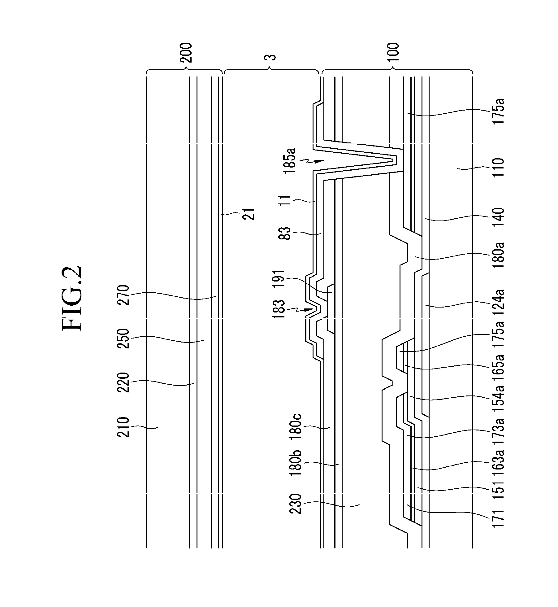
[0046]In drawings, the thickness of layers and regions is exaggerated for clarity. It is to be noted that when a layer is referred to as being “on” another layer or substrate, it can be directly formed on another layer or substrate or can be formed on another layer or substrate through a third layer interposed therebetween. Like constituent elements are denoted by like reference numerals denotes throughout the specification.

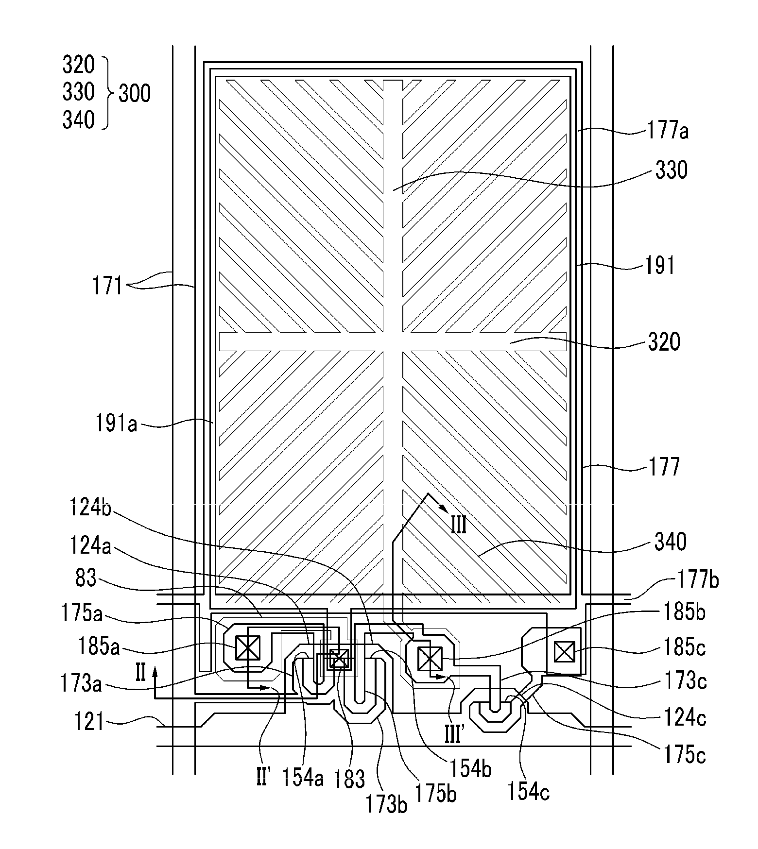
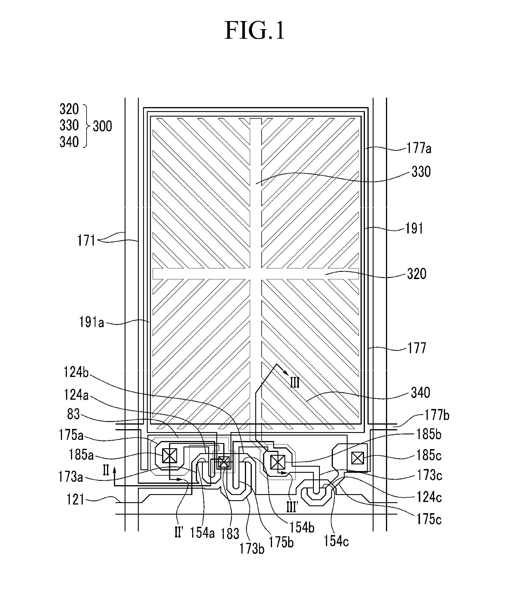
[0047]FIG. 1 is a layout view of a liquid crystal display according to an exemplary emb...


PUM

PropertyMeasurementUnit
voltage V2aaaaaaaaaa
liquidaaaaaaaaaa
response speedaaaaaaaaaa

Abstract

A liquid crystal display and a manufacturing method are provided. A liquid crystal display according to an exemplary embodiment of the present invention includes: a first substrate; a second substrate facing the first substrate; a liquid crystal layer interposed between the first substrate and the second substrate, and including liquid crystal molecules; a first electrode positioned on the first substrate; an insulating layer positioned on the first electrode; a second electrode positioned on the insulating layer; and a third electrode positioned on the second substrate, wherein the second electrode includes a plurality of branches and a slit between neighboring ones of the branches, and a width of the slit is more than about two times to less than about five times a width of its corresponding branches.

Description

CROSS-REFERENCE TO RELATED APPLICATION[0001]This application is a divisional application of U.S. application Ser. No. 13 / 237,798 filed on Sep. 20, 2011 which claims priority to, and the benefit of, Korean Patent Application No. 10-2011-0050195 filed in the Korean Intellectual Property Office on May 26, 2011, the entire contents of which are incorporated herein by reference.BACKGROUND OF THE INVENTION[0002](a) Field of the Invention[0003]Embodiments of the present invention relate generally to liquid crystal displays. More specifically, embodiments of the present invention relate to liquid crystal displays having reduced distortion and improved response speed.[0004](b) Description of the Related Art[0005]A liquid crystal display is one of the types of flat panel display devices that has found wide use. The liquid crystal display commonly includes two display panels where field generating electrodes such as a pixel electrode and a common electrode are formed, and a liquid crystal laye...

Claims


Application Information

Patent Timeline
Patent Type & Authority Applications(United States)
IPC IPC(8): G02F1/1343
CPCG02F1/134336G02F1/1393G02F1/13624G09G2320/0252G09G2300/043G09G2300/0426G09G3/364G02F1/13439G02F2001/134381G02F1/134381G02F1/1343
Inventor HONG, SEUNG HOKWON, OH JEONGLEE, HYEOK JIN
Owner SAMSUNG DISPLAY CO LTD
Why Eureka
Try Eureka