Adjusting Control Gate Overdrive Of Select Gate Transistors During Programming Of Non-Volatile Memory

a technology of select gate transistor and programming memory, which is applied in the direction of digital storage, semiconductor devices, instruments, etc., can solve the problems of various challenges in the operation of such memory devices

Active Publication Date: 2014-10-02
SANDISK TECH LLC
View PDF4 Cites 12 Cited by
  • Summary
  • Abstract
  • Description
  • Claims
  • Application Information

AI Technical Summary

Problems solved by technology

However, various challenges are prese

Method used


Image

  • Adjusting Control Gate Overdrive Of Select Gate Transistors During Programming Of Non-Volatile Memory
  • Adjusting Control Gate Overdrive Of Select Gate Transistors During Programming Of Non-Volatile Memory
  • Adjusting Control Gate Overdrive Of Select Gate Transistors During Programming Of Non-Volatile Memory

Examples


Embodiment Construction

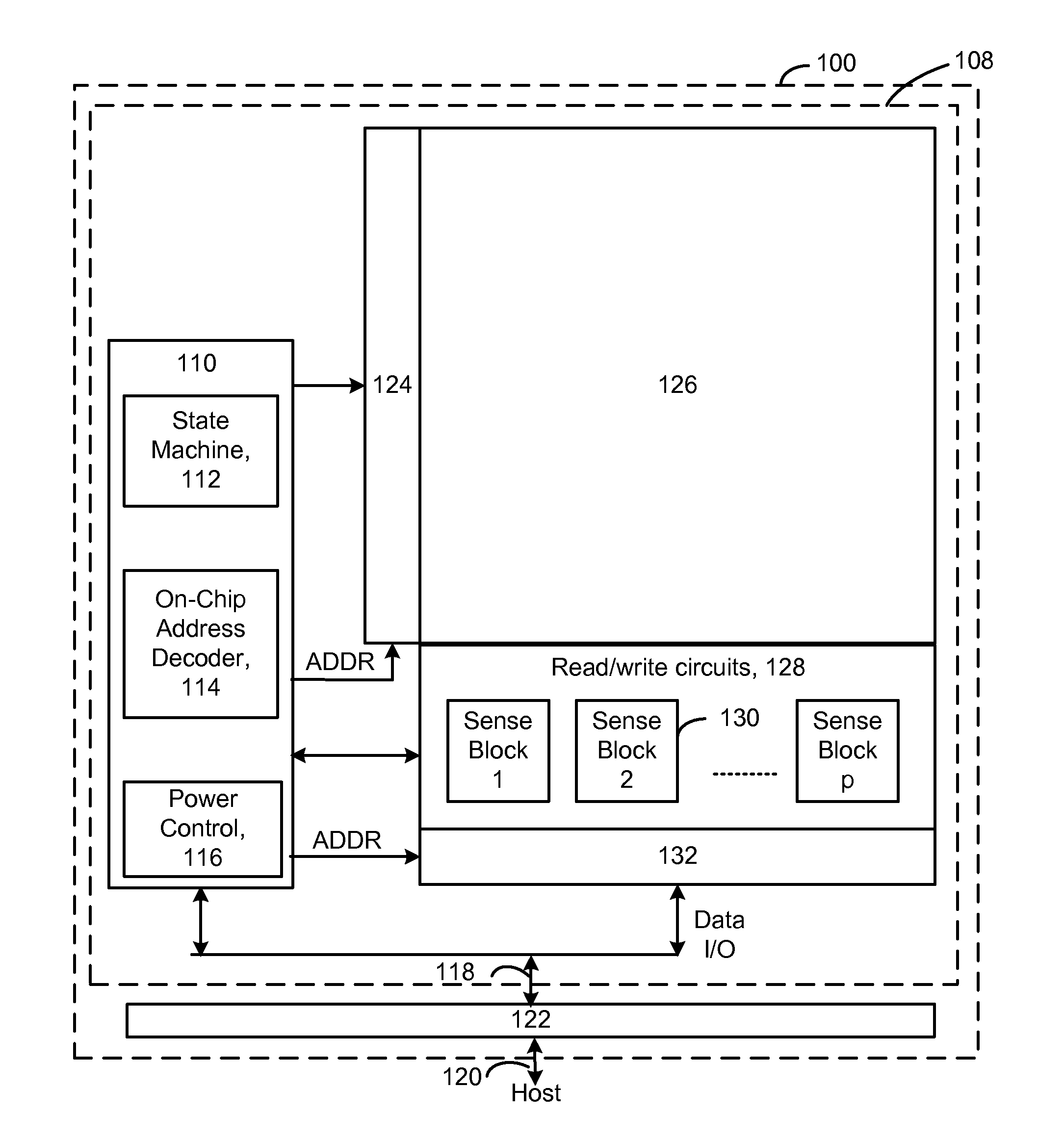
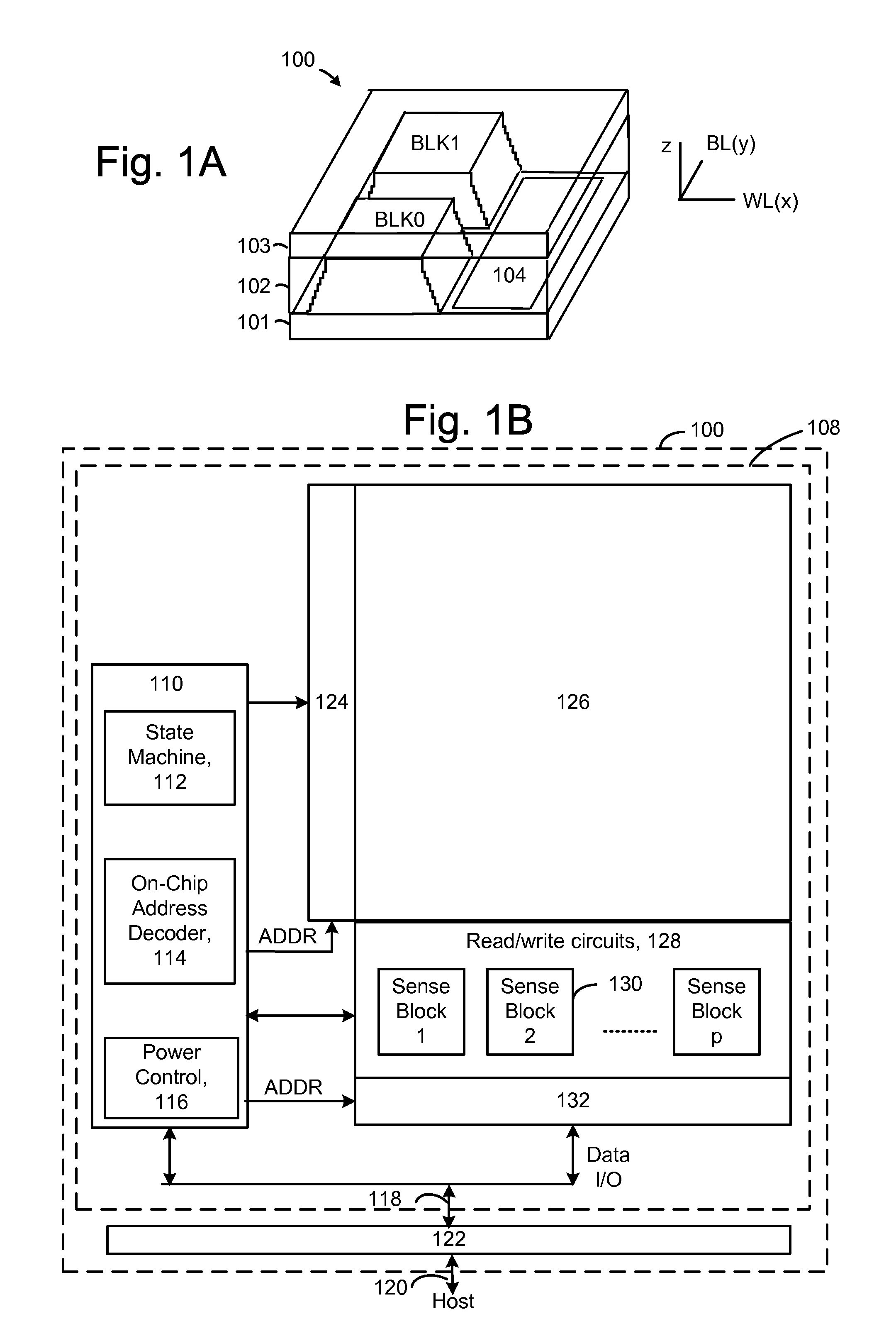
[0049]Techniques are provided for improving the operation of select gate transistors in a memory device such as a 2D or 3D NAND memory device. In particular, the operation of drain-end select gate (SGD) transistors during a programming operation is improved by avoiding or reducing a decrease in a window of acceptable control gate voltages which would otherwise occur. Such a decrease would compromise the ability to program and inhibit the memory cells.

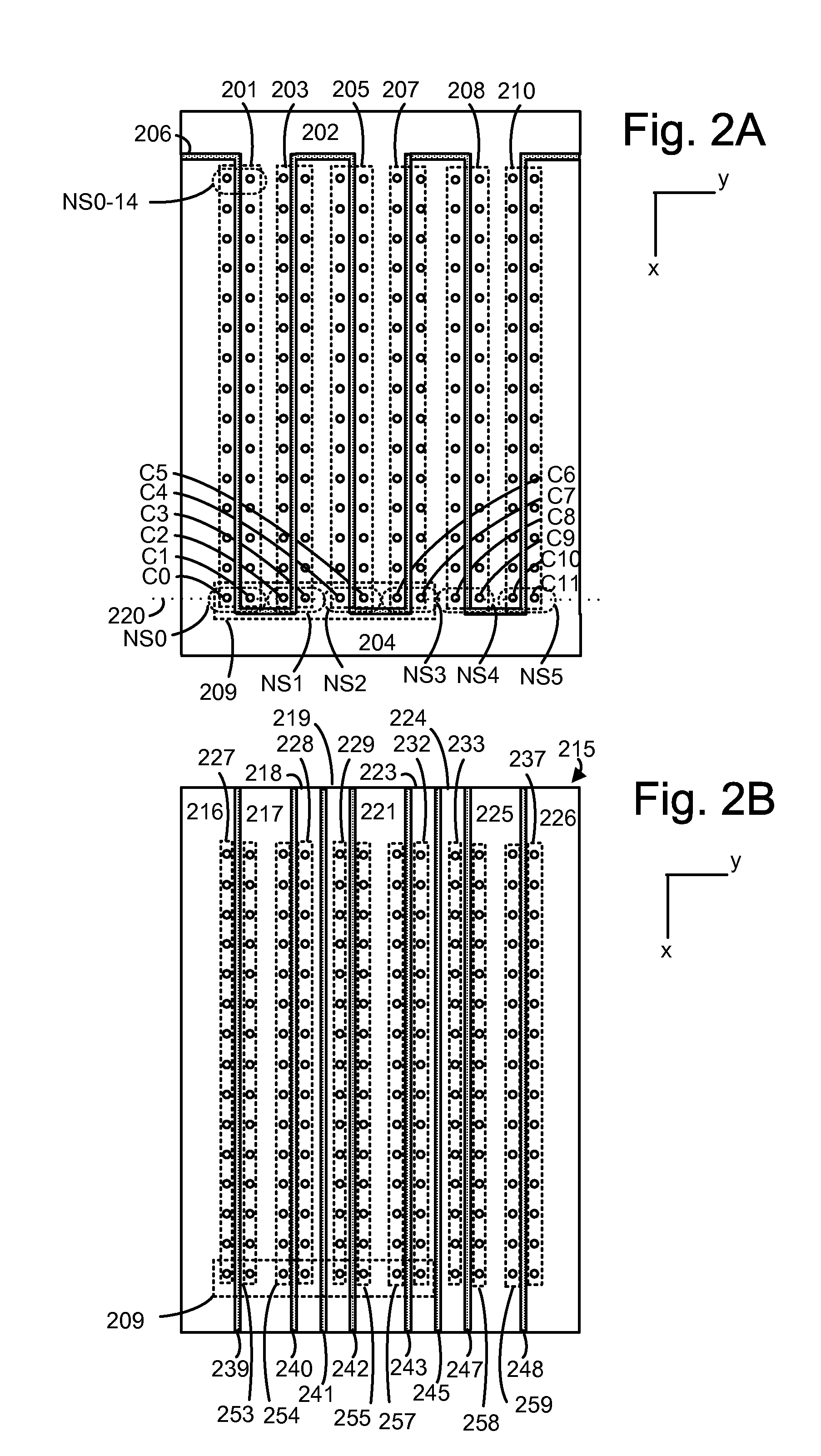
[0050]In a NAND string, an SGD transistor is provided between the memory cells and a bit line. In a programming operation, a common Vsgd is provided to the SGD transistors of a set of NAND strings, where the Vsgd has to be within a specified window or range in order for a programming operation to be successful. To program a memory cell in a selected string, the drain end of the string is connected to a bit line voltage Vbl_sel which is grounded (0 V) or set to a relatively low non-zero voltage which allows programming to occur in a slow...


PUM


Abstract

In a 3D stacked non-volatile memory device, multiple smaller drain-end selected gate (SGD) transistors replace one larger SGD transistor. The SGD transistors have different control gate overdrive voltages so that, during a programming operation, a discontinuous channel potential is created in an inhibited NAND string. The SGD transistor closest to the bit line has a lower control gate overdrive voltage so that the channel potential under it is lower, and the next SGD transistor has a higher control gate overdrive voltage so that the channel potential under it is higher. The different control gate overdrive voltages can be provided by programming different threshold voltages, or by providing different control gates voltages, for the SGD transistors. Undesirable reductions in a Vsgd window due to drain-induced barrier lowering can be avoided.

Description

CROSS-REFERENCE TO RELATED APPLICATIONS[0001]This is a non-provisional patent application which claims the benefit of U.S. provisional patent application No. 61 / 807,716, filed Apr. 2, 2013 and incorporated herein by reference.BACKGROUND OF THE INVENTIONBackground[0002]The present technology relates to techniques for programming in a 3D non-volatile memory device and to the construction of such a device.[0003]Recently, ultra high density storage devices have been proposed using a 3D stacked memory structure sometimes referred to as a Bit Cost Scalable (BiCS) architecture. For example, a 3D NAND stacked memory device can be formed from an array of alternating conductive and dielectric layers. A memory hole is drilled in the layers to define many memory layers simultaneously. A NAND string is then formed by filling the memory hole with appropriate materials. A straight NAND string extends in one memory hole, while a pipe- or U-shaped NAND string (P-BiCS) includes a pair of vertical col...

Claims


Application Information

Patent Timeline
IPC IPC(8): G11C16/12
CPCG11C16/12G11C11/5628G11C16/10G11C16/3427G11C16/0483H10B41/10H10B41/35H10B43/10H10B41/27H10B43/35H10B43/27G11C16/0475H01L29/4983
Inventor DONG, YINGDAHIGASHITANI, MASAAKI
Owner SANDISK TECH LLC
Why Eureka
Try Eureka