
Eureka
For R&D, Eureka makes reading and utilizing patents & technical documents easy.
Eureka AIR
Designed for self-driven R&D workflows. Generate viable solutions, solve complex R&D challenges, empower your innovation with AI.

Eureka Materials
Designed for material experts only. Revolutionize your material R&D, from search, analyze, to developing new materials.

TechResearch
Generate reliable direction feasibility study reports for your R&D in just a few steps.

TechSeek
Discover and master advanced knowledge NOW. Basics, ideas, possibilities, all at once.

TechMind
As an expert in R&D Theories, TechMind can generates customized viable solutions instantly.

TechRisk
Analyze your overall solution with one click, know your potential R&D risks in advance.

TechMonitor
Get weekly tech updates, stay abreast of the latest tech innovations and key insights.
Low energy collimated ion milling of semiconductor structures
a technology of collimated ion milling and semiconductor structure, which is applied in the direction of semiconductor/solid-state device testing/measurement, measurement devices, instruments, etc., can solve the problems of device or structure shift, device or structure damage, etc., and achieve the effect of minimizing surface amorphization
- Summary
- Abstract
- Description
- Claims
- Application Information
AI Technical Summary
Benefits of technology
Problems solved by technology
Method used
Image

Examples
Embodiment Construction
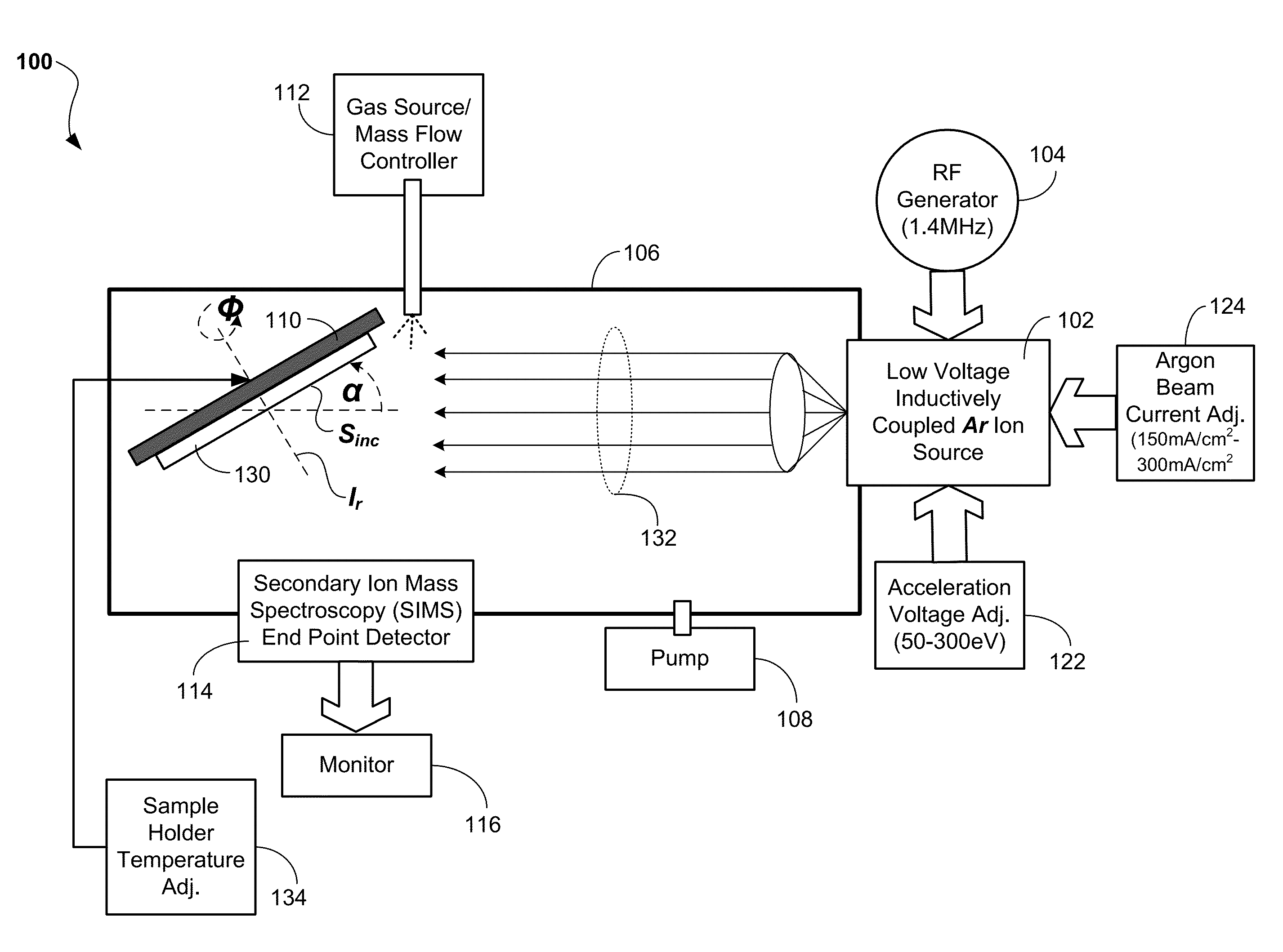
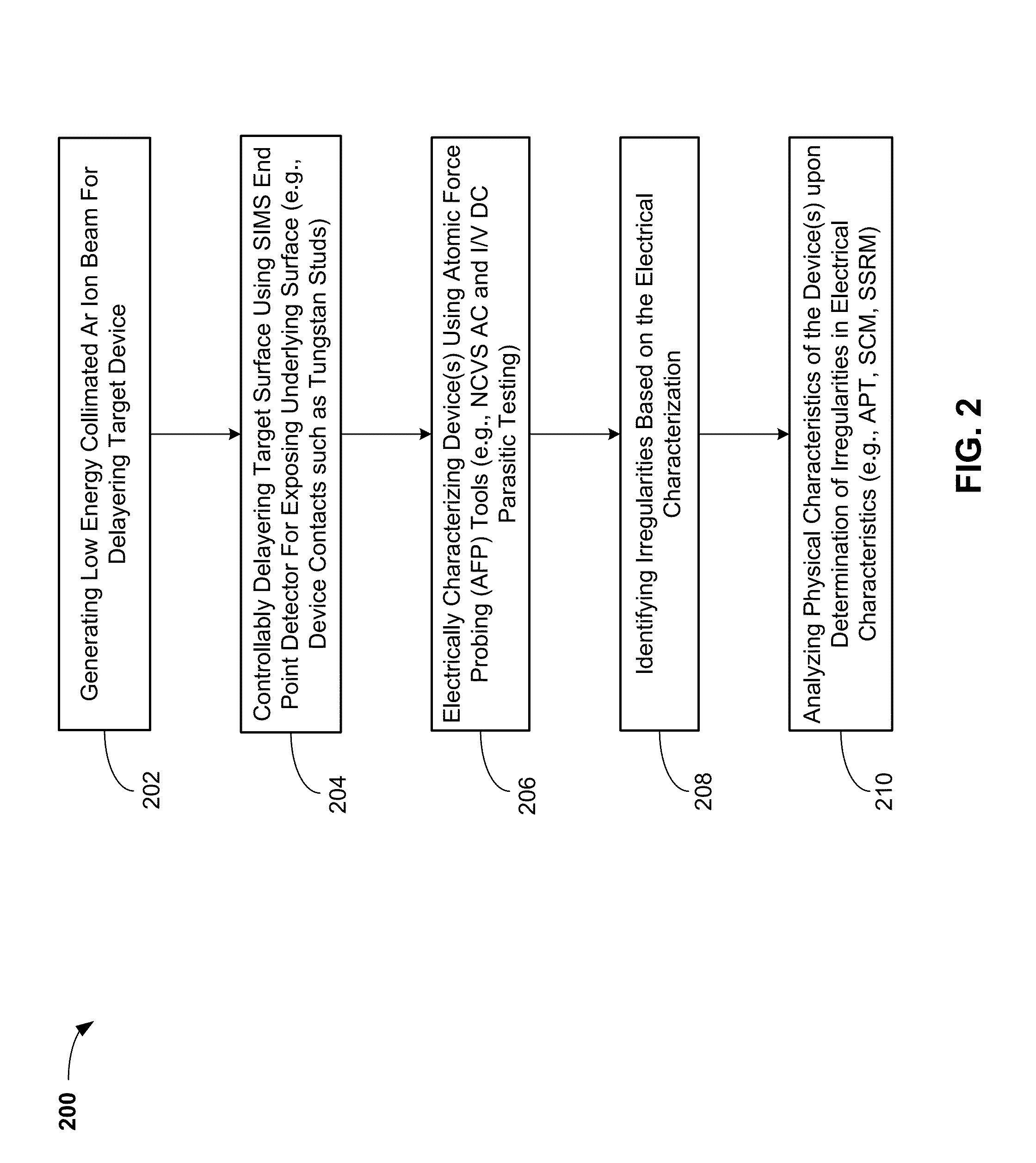
[0013]The following one or more exemplary embodiments describe a low energy ion beam milling apparatus and method utilized for the purpose of delayering the surfaces of semiconductor devices for subsequent testing and characterization of such devices. The delayering of various surfaces of semiconductor devices, particularly three-dimensional semiconductor devices such as FinFet transistor devices, may inadvertently introduce defects and unwanted artifacts within the devices. For example, a high-energy 500 eV focused gallium ion beam may, during the milling and delayering process of a FET device, cause a shift in the threshold voltage (Vt) of the FET device. Additionally, the high-energy ion beam may alter dopant density or dopant distribution. In all such cases, the device may be characterized incorrectly as a result of the induced irregularities or defects that are inadvertently introduced into the semiconductor device under tests based on the ion beam milling process.
[0014]Referri...
PUM
 Abstract
Description
Claims
Application Information
 - R&D Engineer
- R&D Manager
- IP Professional
- Industry Leading Data Capabilities
- Powerful AI technology
- Patent DNA Extraction
Browse by: Latest US Patents, China's latest patents, Technical Efficacy Thesaurus, Application Domain, Technology Topic, Popular Technical Reports.
© 2024 PatSnap. All rights reserved.Legal|Privacy policy|Modern Slavery Act Transparency Statement|Sitemap|About US| Contact US: help@patsnap.com