Luminance measurement method, luminance measurement device, and image quality adjustment technique using the method and device

Active Publication Date: 2014-10-09
IIX
View PDF5 Cites 16 Cited by
  • Summary
  • Abstract
  • Description
  • Claims
  • Application Information

AI Technical Summary

Benefits of technology

[0033]According to the present invention, even if pixel images of a display panel overlap each other on an imaging surface of a camera, it is p

Problems solved by technology

It is known that display panels such as liquid crystal panels and organic EL panels exhibit display unevenness (luminance unevenness and color unevenness) due to variations in manufacturing.
Also, color unevenness occurs if the relative brightness relationship among R, G, and B in each pixe

Method used


Image

  • Luminance measurement method, luminance measurement device, and image quality adjustment technique using the method and device
  • Luminance measurement method, luminance measurement device, and image quality adjustment technique using the method and device
  • Luminance measurement method, luminance measurement device, and image quality adjustment technique using the method and device

Examples


Example

Embodiment 1

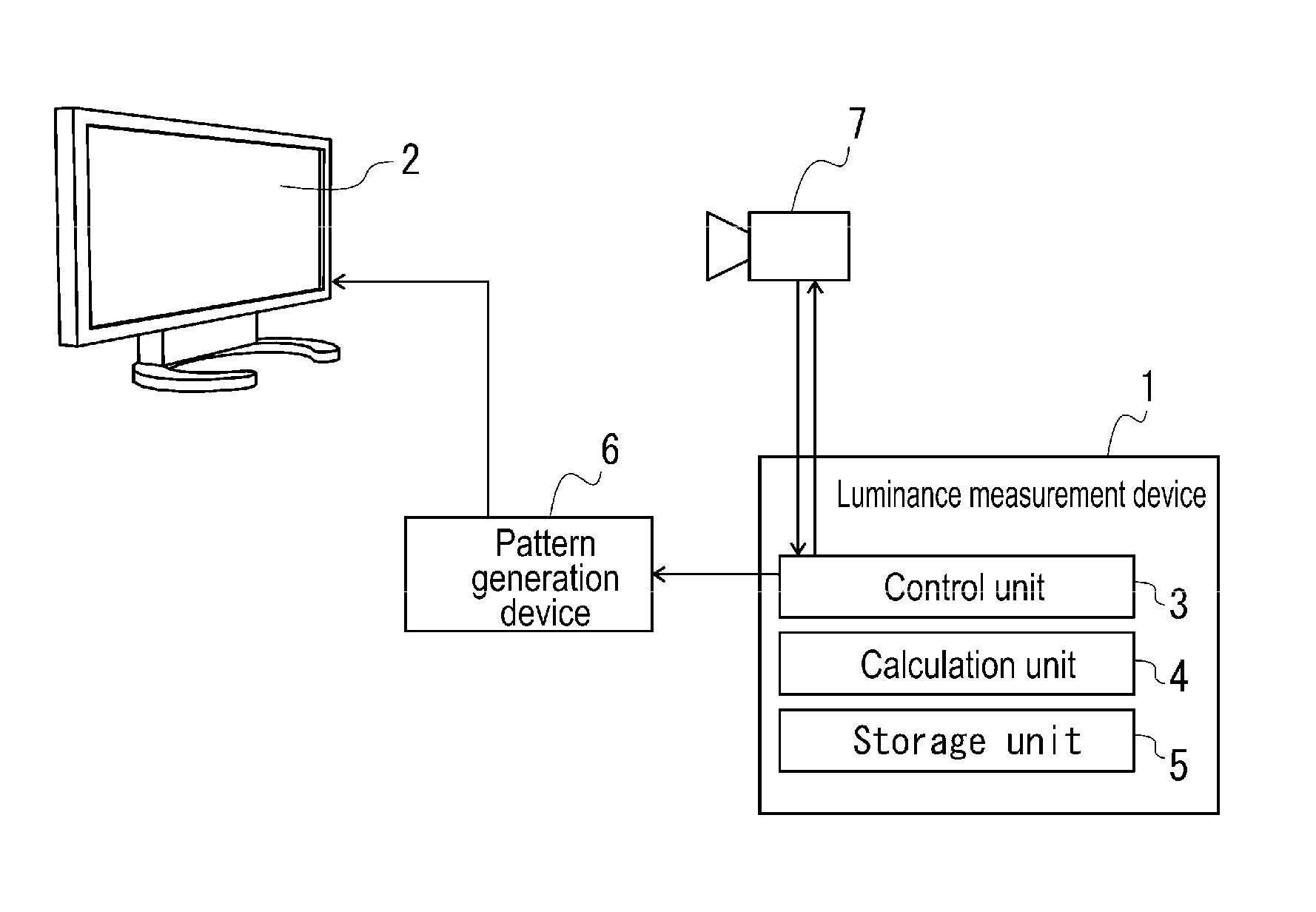
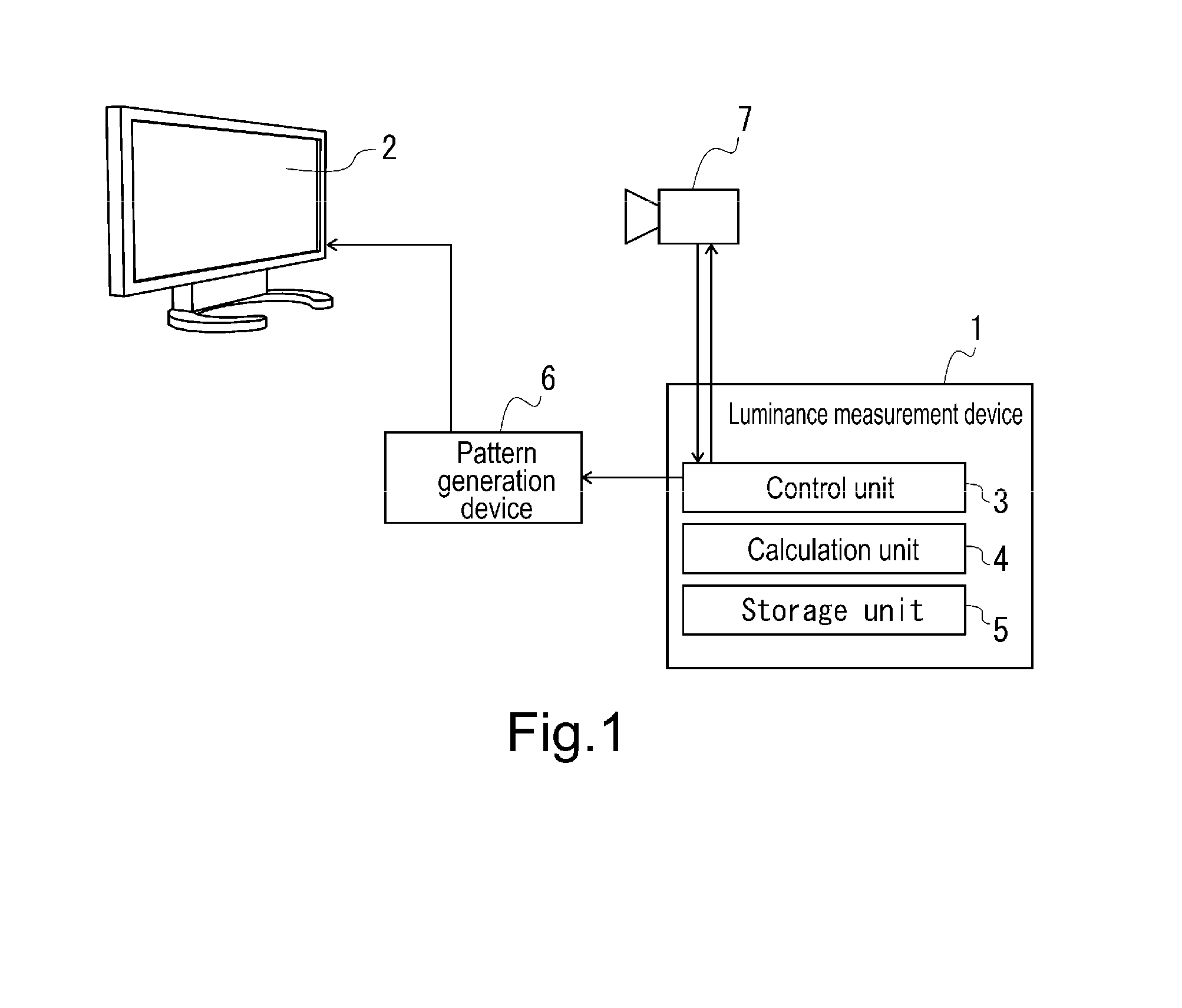
[0045]FIG. 1 illustrates a luminance measurement device according to the present embodiment. This luminance measurement device 1 measures the luminance of all pixels of an organic EL panel 2 (each pixel of the organic EL panel 2 is made up of R, G, and B subpixels, and it is assumed in the present invention that “pixel” encompasses such subpixels), and includes a control unit 3, a calculation unit 4, and a storage unit 5. The control unit 3 controls display of the organic EL panel 2 via a pattern generation device 6, and controls imaging by a monochrome solid-state imaging camera 7 that is disposed facing the organic EL panel 2. The calculation unit 4 performs various types of calculation based on the image that was imaged by the camera 7 or the like, and the storage unit 5 stores the imaging result of the camera 7 and the calculation results of the calculation unit 4.

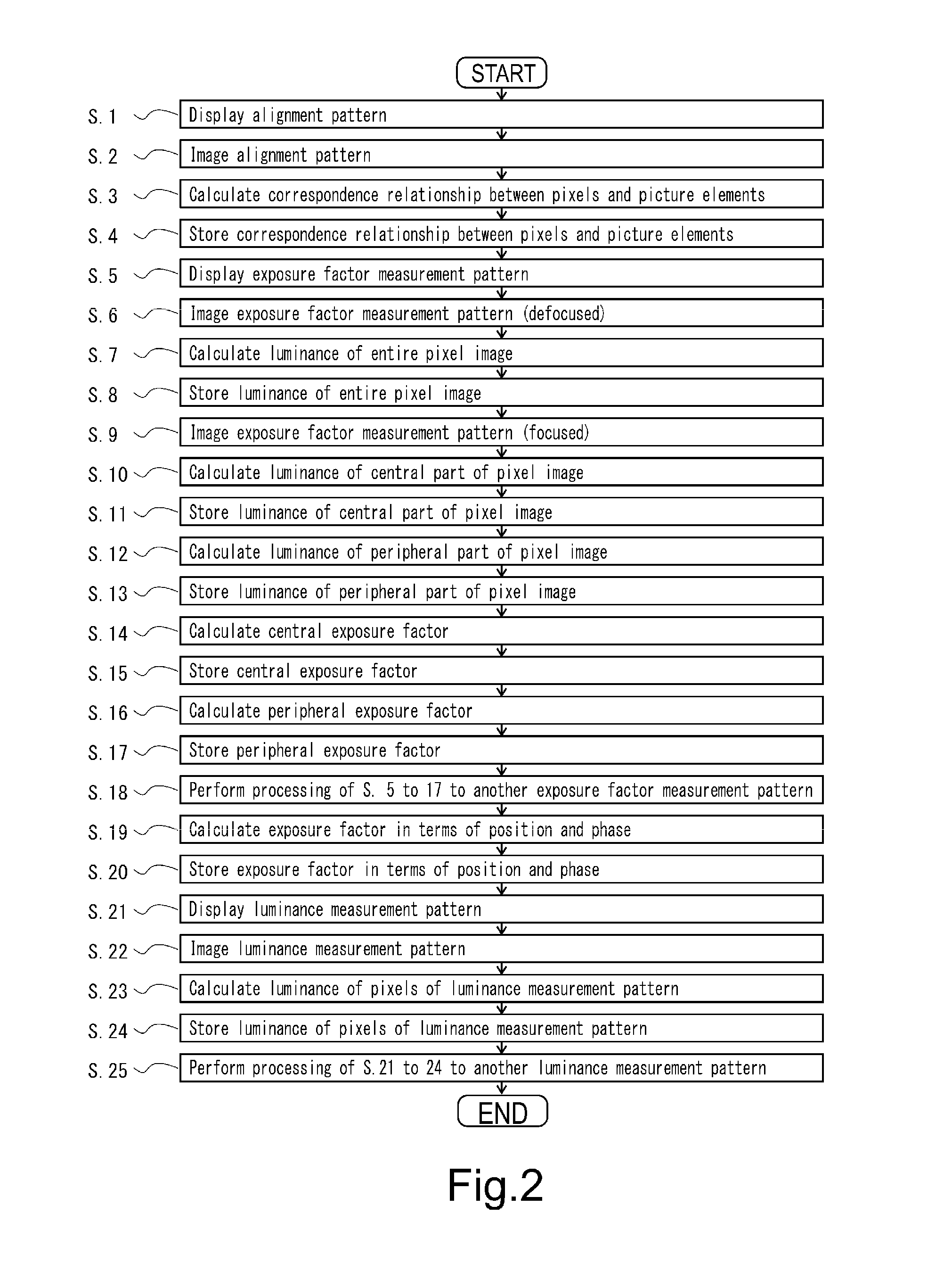
[0046]As illustrated in FIG. 2, when the luminance measurement device 1 measures the luminance of pixels...

Example

Embodiment 2

[0073]FIG. 9 illustrates a correction data generation device according to the present embodiment. This correction data generation device 10 is configured by additionally connecting a ROM writer 11 to the luminance measurement device 1 according to Embodiment 1. As shown in FIG. 109, the correction data generation device 10, like the luminance measurement device 1, measures the luminance of all pixels of the organic EL panel 2 (steps 1 to 25), and then the calculation unit 4 generates correction data for reducing display unevenness (luminance unevenness) of the organic EL panel 2 on the basis of the luminance of each pixel (step 26). The generated correction data is written in a ROM (nonvolatile memory) 12 by the ROM writer 11 (step 27), and an image quality adjustment type organic EL panel 14 is manufactured by an image quality adjustment circuit 13 in which this ROM 12 is provided being mounted on the organic EL panel 2 (step 28).

[0074]In the image quality adjustment ty...


PUM


Abstract

Provided is a luminance measurement method for accurately measuring luminance of each pixel even if pixel images of a display panel overlap each other on an imaging surface of a camera. A central exposure factor indicating luminance of the central part of the pixel image is calculated on the basis of an output of a picture element corresponding to the central part. A peripheral exposure factor indicating luminance of the peripheral part of the pixel image is calculated on the basis of an output of picture elements corresponding to the peripheral part of the pixel image is calculated, all pixels of the display panel are sorted into a plurality of groups, sequentially turned on one group after another, and imaged by the camera, and the luminance of all the pixels of the display panel is calculated based on this imaged image, the central exposure factor, and the peripheral exposure factor.

Description

CROSS REFERENCE TO RELATED APPLICATIONS[0001]This is a continuation in part application of U.S. patent application Ser. No. 14 / 069,834 filed on Nov. 1, 2013, which is a continuation application of PCT application serial number PCT / JP2013 / 060659, filed on Apr. 8, 2013, the entire contents of which are incorporated herein by reference.TECHNICAL FIELD [0002]The present invention relates to a luminance measurement method and a luminance measurement device that measure the luminance of pixels of a display panel, and an image quality adjustment technique using the method and the device.BACKGROUND ART[0003]It is known that display panels such as liquid crystal panels and organic EL panels exhibit display unevenness (luminance unevenness and color unevenness) due to variations in manufacturing. When each pixel of the display panel has R, G, and B subpixels, luminance unevenness occurs if the absolute brightness relationship differs between adjacent pixels even though the relative brightness...

Claims


Application Information

Patent Timeline
IPC IPC(8): H04N17/00
CPCH04N17/00G02F1/1339H04N17/02H01L23/498H01L23/00H01L2924/0002G01J3/506H04N9/3182H04N9/3194G09G3/006G09G2300/0452G09G2320/0233G09G2320/0242G09G2320/0693G02F1/1309H01L2924/00
Inventor MURASE, HIROSHI
Owner IIX
Why Eureka
Try Eureka