Semiconductor device and electronic device including the same

Active Publication Date: 2014-10-09
SK HYNIX INC
View PDF4 Cites 38 Cited by
  • Summary
  • Abstract
  • Description
  • Claims
  • Application Information

AI Technical Summary

Benefits of technology

[0013]Various embodiments are directed to a semiconductor device in which impurities are implanted into sidewalls of a variable resistance layer to limit an area where a current path is generated, and one or few c

Problems solved by technology

In other words, it may be difficult to regenerate the current path C at a specific location of the variable resistance layer 20.
Therefore, the resistance switching characteristics may become n

Method used


Image

  • Semiconductor device and electronic device including the same
  • Semiconductor device and electronic device including the same
  • Semiconductor device and electronic device including the same

Examples


first embodiment

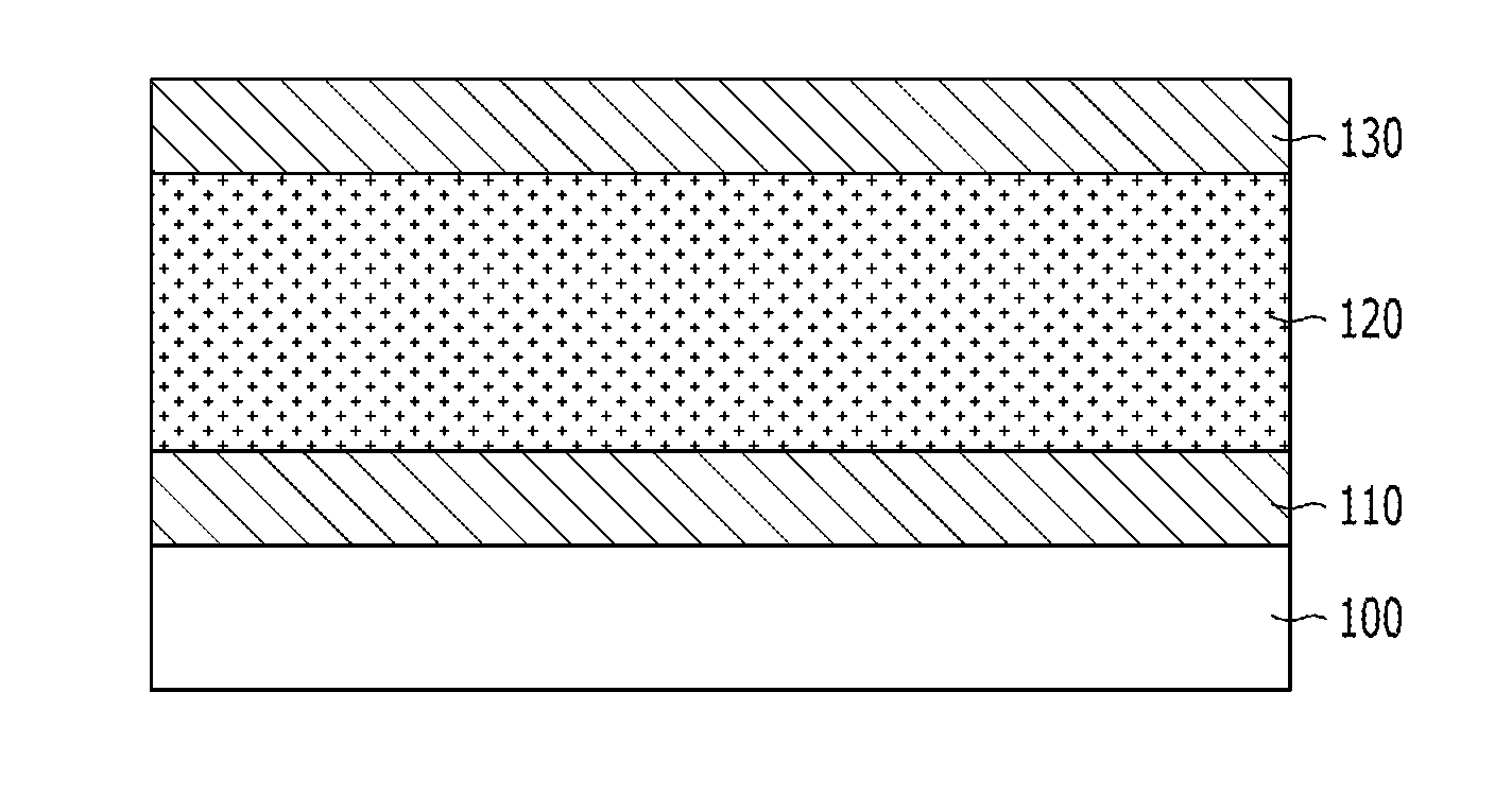
[0039]Referring to FIG. 3C, the semiconductor device in accordance with the first embodiment may include the first conductive layer pattern 110A over the substrate 100, the second conductive layer pattern 130A spaced from the first conductive layer pattern 110A, the variable resistance layer pattern 120A interposed between the first and second conductive layer patterns 110A and 130A, and the impurity-doped layer 140 surrounding side surfaces of the variable resistance layer pattern 120A.

[0040]The impurity-doped layer 140, which is doped with one or more of Si and Ge, has a higher resistance value than the variable resistance layer pattern 120A, and may include silicate or silicide. The variable resistance layer pattern 120A may include a material of which electric resistance is changed by migration of oxygen vacancies or ions or a material of which electric resistance is changed by phase change. The width D2 of the variable resistance layer pattern 120A is smaller than the width D1 ...

second embodiment

[0042]Referring to FIG. 4, first conductive layer patterns 110A of the semiconductor device in accordance with the second embodiment may be extended in parallel to each other in a first direction, and second conductive layer patterns 130A may be extended in parallel to each other in a second direction crossing the first direction and the conductive layer patterns 110A. At each of the intersections between the first and second conductive layer patterns 110A and 130A, the variable resistance layer pattern 120A and the impurity-doped layer 140 surrounding side surfaces of the variable resistance layer pattern 120A may be arranged.

third embodiment

[0043]Referring to FIG. 5, a selecting element layer 150 may be interposed between the first conductive layer pattern 110A and the variable resistance layer pattern 120A of the semiconductor device in accordance with the The selecting element layer 150 may include a transistor which may be turned on / off or a diode which is configured to pass a current only in one direction. In addition, the selecting element layer 150 may include an asymmetrical tunnel barrier having a nonlinear current-voltage characteristic, a metal-insulator transition (MIT) element which undergoes a transition from an insulator to a metal at a specific critical temperature such that the electric resistance thereof rapidly changes, or an ovonic switching element which performs a switching operation at a specific threshold voltage. In an embodiment, the selecting element layer 150 may be interposed between the variable resistance layer 120A and the second conductive layer pattern 130A.

[0044]FIGS. 6A to 6C are cro...


PUM


Abstract

A semiconductor device includes a first conductive layer, a second conductive layer spaced from the first conductive layer, a variable resistance layer interposed between the first and second conductive layers, and an impurity-doped layer provided over a side surface of the variable resistance layer. The variable resistance layer has a smaller width than the first and the second conductive layers.

Description

CROSS-REFERENCE TO RELATED APPLICATION[0001]The present application claims priority Korean Patent Application No. 10-2013-0037371, filed on Apr. 5, 2013, which is incorporated by reference herein in its entirety.BACKGROUND[0002]1. Field[0003]Exemplary embodiments relate to a semiconductor device and an electronic device including the same, and more particularly, to a semiconductor device including a variable resistance layer which is capable of switching between two different resistance states in response to an applied voltage or current, and an electronic device including the same.[0004]2. Description of the Related Art[0005]A variable resistance memory device, of which the resistance changes according to an external stimulus, switches between two or more resistance states so as to store data, and includes a resistive random access memory (ReRAM), a phase change RAM (PCRAM), a spin transfer torque-RAM (STT-RAM) and the like. In particular, the variable resistance memory device may ...

Claims


Application Information

Patent Timeline
IPC IPC(8): H01L45/00G11C13/00
CPCG11C13/0069H01L45/145H01L45/085H01L45/1233G11C13/0004H01L45/144H01L45/08H01L45/06G11C2213/55G11C13/0007H01L27/2463H01L45/147H01L45/1293H01L45/146H10B63/80H10N70/245H10N70/24H10N70/231H10N70/8616H10N70/826H10N70/8836H10N70/8828H10N70/8833H10N70/20
Inventor KIM, BEOM-YONGLEE, KEE-JEUNGKIM, WAN-GEEKIM, HYO-JUNE
Owner SK HYNIX INC
Why Eureka
Try Eureka