Phase-change memory device having phase-change region divided into multi layers and operating method thereof

a phase-change memory and multi-layer technology, applied in semiconductor devices, digital storage, instruments, etc., can solve problems such as difficulty in accurately implementing multi-levels, and achieve the effect of small resistivity and lower crystallization ra

Inactive Publication Date: 2014-10-09
SK HYNIX INC
View PDF11 Cites 12 Cited by
  • Summary
  • Abstract
  • Description
  • Claims
  • Application Information

AI Technical Summary

Benefits of technology

[0008]According to an aspect of an exemplary embodiment, a phase-change memory device includes a first phase-change material layer to which a current is provided from a heating electrode, and a second phase-change material layer formed with continuity to the first phase-change material layer and having a different width from the first phase-change material layer, and to which a current is provided from the heating electrode. The second phase-change material layer may include a material having smaller resistivity and a lower crystallization rate than the first phase-change material layer.

Problems solved by technology

However, in the phase-change memory device of the related art, as shown in FIG. 1, since a phase-change material layer is formed to overlap a bit line 20 and heating electrodes BEC1, BEC2, and BEC3 which are in contact with one phase-change line 10 are densely formed, it is difficult to implement accurately multi levels due to influence of adjacent cells cell1, cell2, and cell3.

Method used


Image

  • Phase-change memory device having phase-change region divided into multi layers and operating method thereof
  • Phase-change memory device having phase-change region divided into multi layers and operating method thereof
  • Phase-change memory device having phase-change region divided into multi layers and operating method thereof

Examples


Embodiment Construction

”.

BRIEF DESCRIPTION OF THE DRAWINGS

[0013]The above and other aspects, features and other advantages of the subject matter of the present disclosure will be more clearly understood from the following detailed description taken in conjunction with the accompanying drawings, in which:

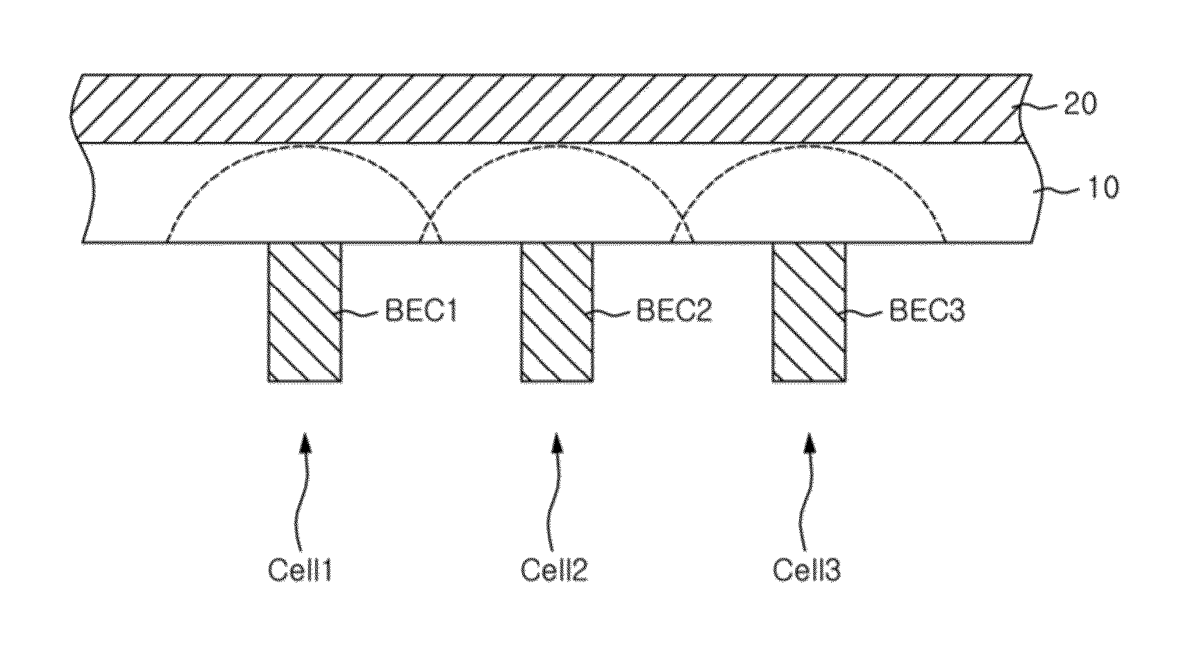
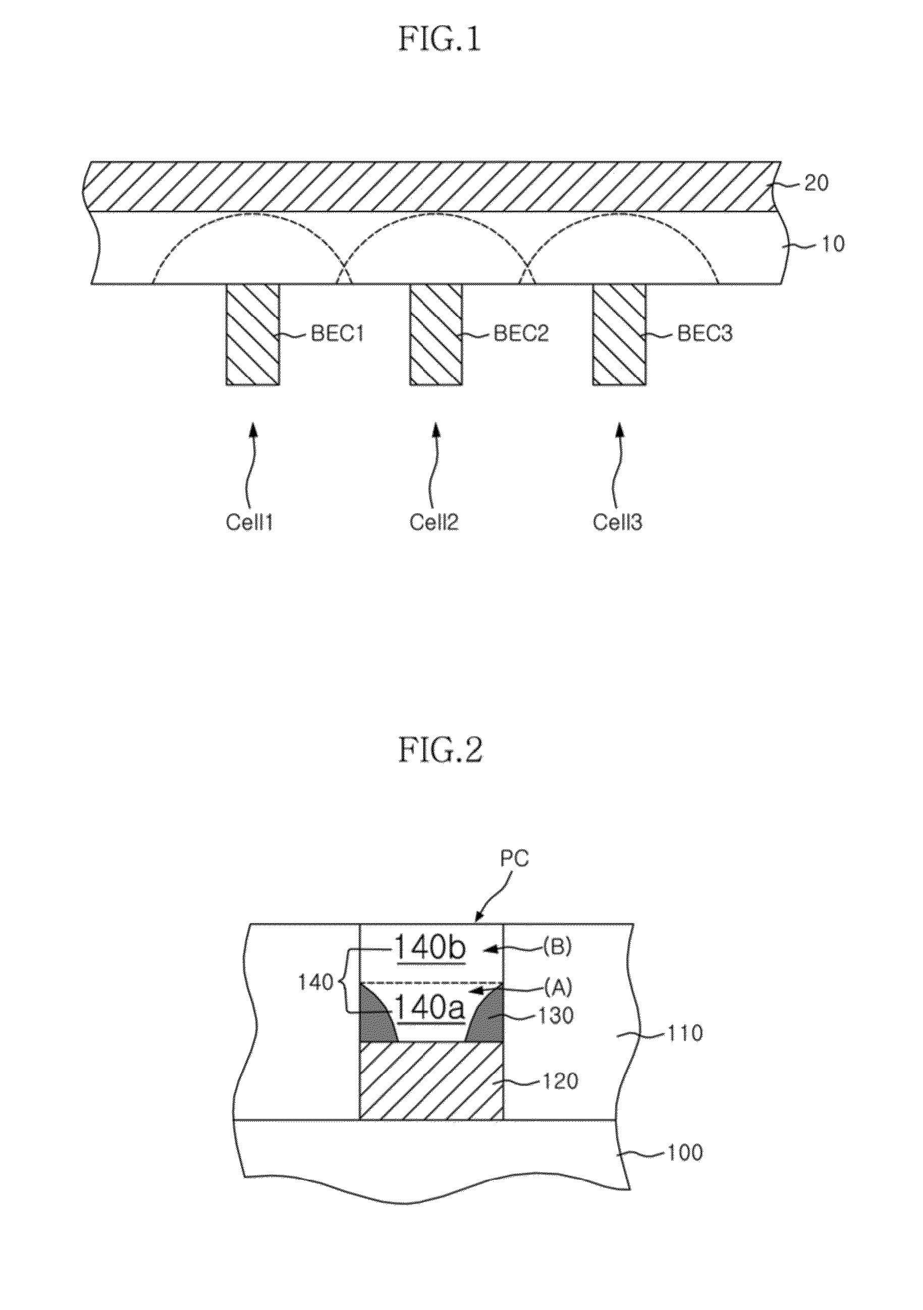
[0014]FIG. 1 is a schematic cross-sectional view illustrating a driving of a general phase-change memory device;

[0015]FIG. 2 is a cross-sectional view illustrating a phase-change memory device according to an exemplary embodiment of the inventive concept;

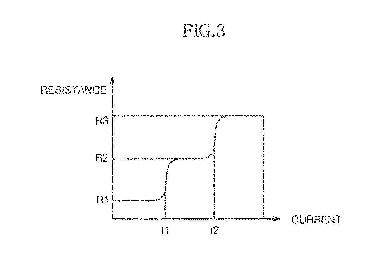
[0016]FIG. 3 is a graph showing a resistance level according to current application in a phase-change memory device according to an exemplary embodiment of the inventive concept;

[0017]FIGS. 4A to 4C are cross-sectional views for processes illustrating a method of manufacturing a phase-change memory device according to an exemplary embodiment of the inventive concept;

[0018]FIG. 5 is a cross-sectional view illustrating a phase-change memory device according ...


PUM


Abstract

A phase-change memory device including a multi-level cell and an operation method thereof are provided. The device includes a first phase-change material layer to which a current is provided from a heating electrode, and a second phase-change material layer formed with continuity to the first phase-change material layer and having a different width from the first phase-change material layer, and to which a current is provided from the heating electrode. The second phase-change material layer includes a material having smaller resistivity and a lower crystallization rate than the first phase-change material layer.

Description

CROSS-REFERENCES TO RELATED APPLICATION[0001]The application is a continuation-in-part of the U.S. patent application Ser. No. 13 / 331,254 filed Dec. 20, 2011 and titled “PHASE-CHANGE MEMORY DEVICE HAVING MULTI-LEVEL CELL AND A METHOD OF MANUFACTURING THE SAME”, which is incorporated here in by reference in its entirety.BACKGROUND OF THE INVENTION[0002]1. Technical Field[0003]The inventive concept relates to a nonvolatile memory device and an operating method thereof, and more particularly, to a phase-change memory device including a multi-level cell and an operating method thereof.[0004]2. Related Art[0005]Research has been conducted on nonvolatile memory devices such as phase-change memory devices to implement a multi-level cell while minimizing modification of a cell shape.[0006]Technology, in which a stepwise write voltage is provided to a bit line of a phase-change memory device to vary a degree of phase-change of a phase-change material, thereby implementing multi levels, has b...

Claims


Application Information

Patent Timeline
Patent Type & Authority Applications(United States)
IPC IPC(8): H01L45/00G11C13/00
CPCH01L45/12G11C13/0004H01L45/06H01L45/1233H01L27/2463H01L45/126H01L45/144H01L45/1683H01L45/1246G11C11/5678G11C13/0069G11C2013/0092H10B63/80H10N70/828H10N70/8413H10N70/231H10N70/8828H10N70/826H10N70/066
Inventor KIM, JIN HYOCKCHAE, SU JINKWON, YOUNG SEOKPARK, HAE CHAN
Owner SK HYNIX INC
Why Eureka
Try Eureka