LED display and manufacturing method thereof

a manufacturing method and light-emitting diode technology, applied in semiconductor/solid-state device manufacturing, semiconductor devices, electrical devices, etc., can solve the problems of difficult to further reduce the thickness or weight, difficult to manufacture led displays, and high cost of oled emitting materials, etc., to achieve easy manufacturing of led displays, light weight, and small size

Active Publication Date: 2014-10-23
LEXTAR ELECTRONICS CORP
View PDF4 Cites 62 Cited by
  • Summary
  • Abstract
  • Description
  • Claims
  • Application Information

AI Technical Summary

Benefits of technology

[0008]The invention is directed to a LED display and a manufacturing method thereof. In the LED display manufacturing method according to this invention, LED chips are provided by a temporary substrate. As such, the LED display can be manufactured easily. Moreover, the LED display manufactured by said method has the advantages of lighter weight, smaller size, lower power consumption, higher contrast, higher response rate, lower cost, and longer lifespan.

Problems solved by technology

However, the liquid crystal display requires an additional backlight module, making it difficult to further reduce the thickness or the weight.
However, the light emitting material of the OLED is expensive, the lifespan of OLED is relatively short, and the manufacturing process of the OLED is complicate.
Therefore, the OLED still cannot replace the LCD and become widely used.

Method used


Image

  • LED display and manufacturing method thereof
  • LED display and manufacturing method thereof
  • LED display and manufacturing method thereof

Examples


Embodiment Construction

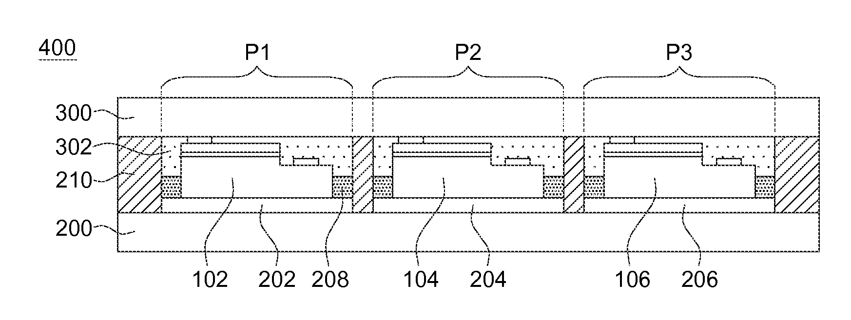
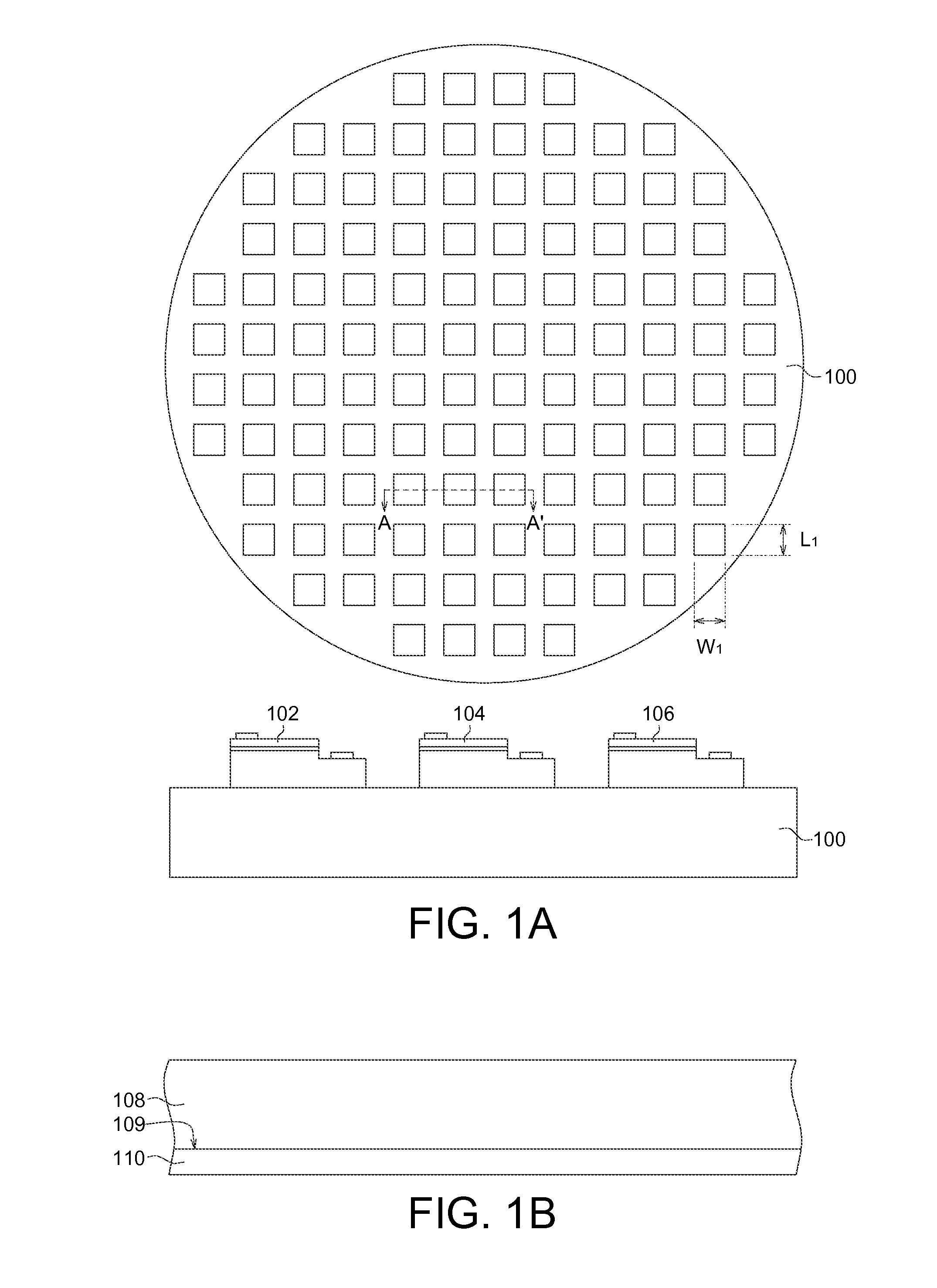
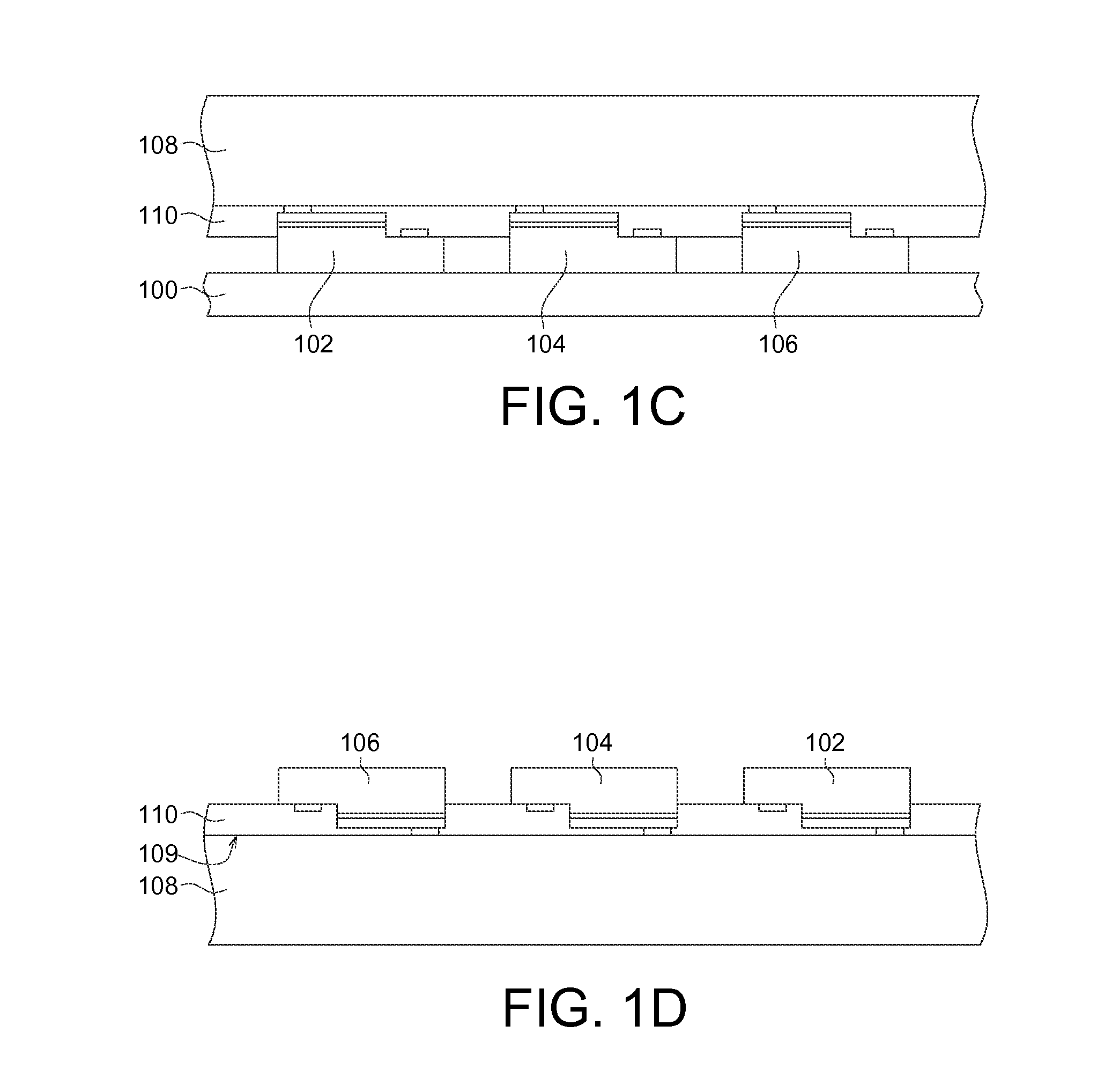
[0014]Referring to FIGS. 1A-1H, a manufacturing method of a LED display according to one embodiment of the invention are schematically shown. For clarity, sizes and relative dimensions of elements in the figures may not be illustrated according to their real sizes and relative dimensions, and some elements and reference numerals may be omitted in some diagrams.

[0015]FIG. 1A shows a top view of a substrate with a plurality of LEDs epitaxially formed thereon and a cross-sectional view along a cross-sectional line A-A′. As shown in FIG. 1A, a substrate (such as a sapphire substrate) 100 has a plurality of LED chips formed thereon. The LED chips comprise a first LED chip 102, a second LED chip 104 and a third LED chip 106. The first, second and third LED chips 102, 104 and 106 are substantially the same, however, the invention is not limited thereto. In one embodiment, a length L1 and a width W1 of each of the first, the second and the third LED chips 102, 104 and 106 are less than or e...


PUM


Abstract

A manufacturing method of a LED display is provided. A temporary substrate is provided, wherein the temporary substrate has a first adhesive layer and a plurality of first, second and third LED chips mounted on the first adhesive layer. A first transparent substrate is provided, the transparent substrate has a plurality of pixels disposed thereon, and each of the pixels comprises a first sub-pixel, a second sub-pixel and a third sub-pixel respectively surrounded by a light-insulating structure. Then, the temporary substrate and the first transparent substrate are bonded together, such that each of the first, second and third LED chips is correspondingly mounted in each of the first sub-pixels, the second sub-pixels and the third sub-pixels. After that, the temporary substrate is removed. A LED display manufactured by said method is also provided.

Description

[0001]This application claims the benefit of Taiwan application Serial No. 102113992, filed on Apr. 19, 2013, the subject matter of which is incorporated herein by reference.BACKGROUND[0002]1. Technical Field[0003]The invention relates in general to a display and a manufacturing method thereof. More particularly, the invention relates to a light emitting diode (LED) display manufacturing method, and a LED display manufactured by said method and capable of emitting lights of multi-wavelengths.[0004]2. Description of the Related Art[0005]Flat-panel displays commonly seen comprise liquid crystal display (LCD) and organic light-emitting diode display (OLED).[0006]Liquid crystal display is the mainstream product, the related technologies have been fully developed, and its price is low. However, the liquid crystal display requires an additional backlight module, making it difficult to further reduce the thickness or the weight.[0007]OLED, which is self-luminous and does not require the ba...

Claims


Application Information

Patent Timeline
Patent Type & Authority Applications(United States)
IPC IPC(8): H01L33/00H01L33/50H01L27/15
CPCH01L33/005H01L33/50H01L27/156H01L25/0753H01L2933/0041H01L21/6835H01L2221/68354H01L2221/68368H01L2221/68381H01L2924/0002H01L33/0093H01L2924/00H01L33/504H01L33/08H01L33/502H01L33/56
Inventor LEE, CHIA-ENHOU, CHIA-HUNG
Owner LEXTAR ELECTRONICS CORP
Why Eureka
Try Eureka