Active device

a technology of active devices and semiconductors, applied in the direction of semiconductor devices, electrical apparatus, transistors, etc., can solve the problems that the field-effect mobility of conventional oxide semiconductor tft is not easy to be further enhanced, and achieve the effect of improving the field-effect mobility

Active Publication Date: 2014-11-06
E INK HLDG INC
View PDF3 Cites 8 Cited by
  • Summary
  • Abstract
  • Description
  • Claims
  • Application Information

AI Technical Summary

Benefits of technology

[0006]Accordingly, the invention is directed to an active device with better field-effect mobility.

Problems solved by technology

However, under its existing architecture, the conventional oxide semiconductor TFT is not easy to further enhance field-effect mobility.

Method used


Image

  • Active device
  • Active device
  • Active device

Examples


Embodiment Construction

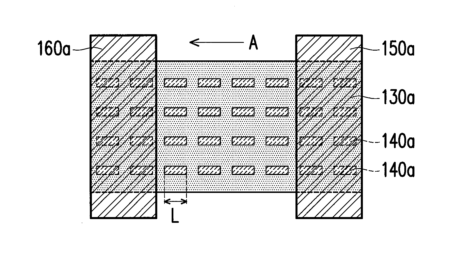
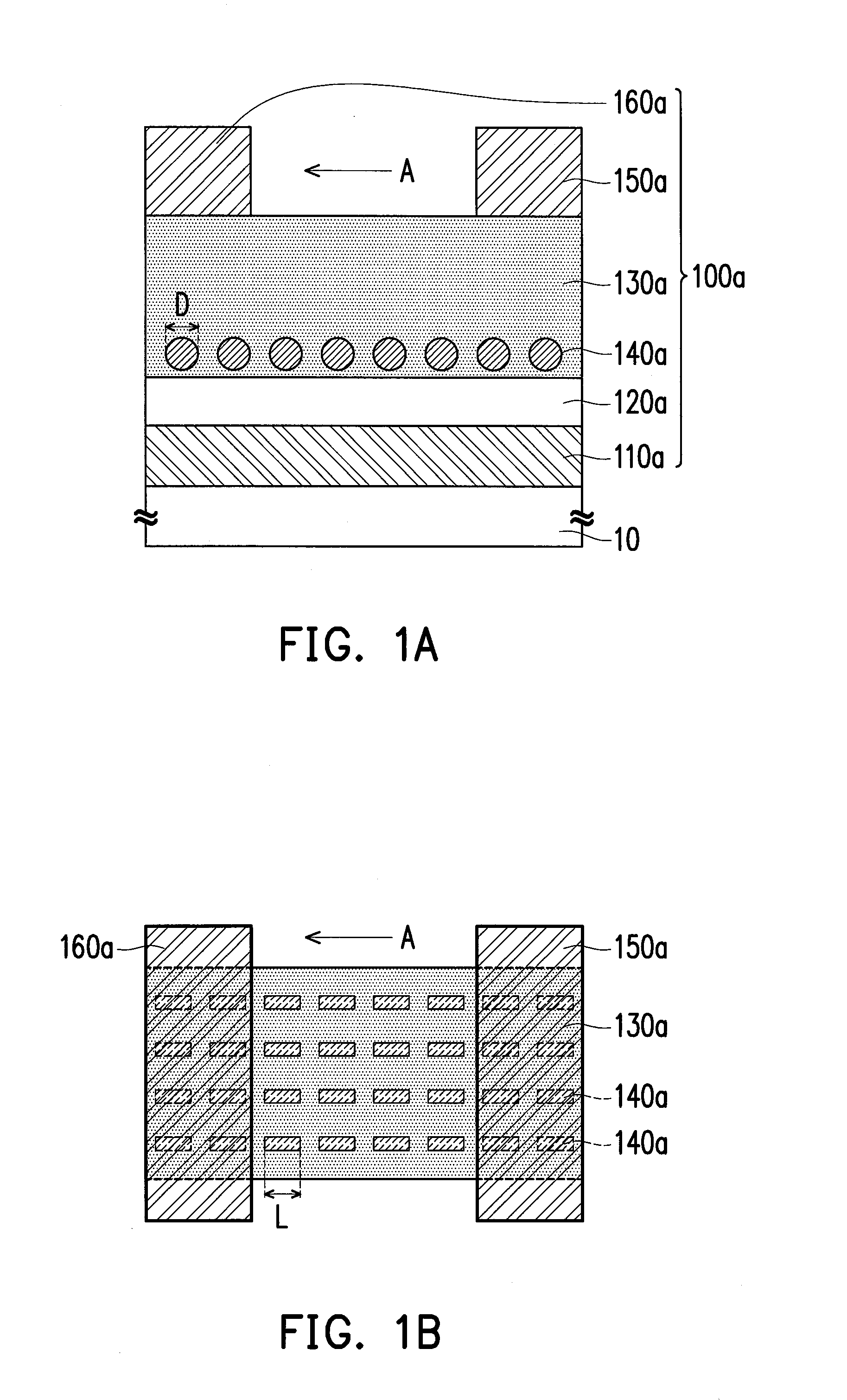
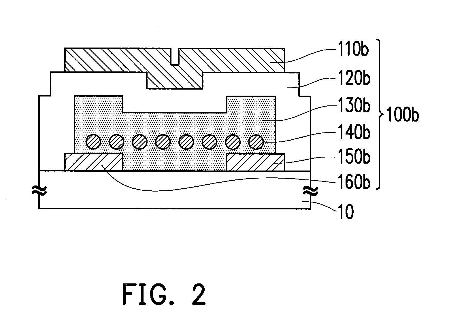
[0023]FIG. 1A is a cross-sectional diagram of an active device according to an embodiment of the invention and FIG. 1B is a top-view diagram illustrating the oxide semiconductor channel layer, the nano conductive wires, the source and the drain in FIG. 1A. Referring to FIGS. 1A and 1B, in the embodiment, an active device 100a is disposed on a substrate 10, in which the material of the substrate 10 is, for example, glass, plastic or other appropriate materials. The active device 100a includes a gate 110a, a gate insulating layer 120a, an oxide semiconductor channel layer 130a, a plurality of nano conductive wires 140a, a source 150a and a drain 160a.

[0024]In more details, in the embodiment, the gate 110a is disposed on the substrate 10, and the gate insulating layer 120a is disposed between the gate 110a and the oxide semiconductor channel layer 130a, in which the gate insulating layer 120a covers the gate 110a. The nano conductive wires 140a are distributed in the oxide semiconduct...


PUM


Abstract

An active device provided by the invention is disposed on a substrate and includes a gate, a gate insulating layer, an oxide semiconductor channel layer, a plurality of nano conductive wires, a source and a drain. The gate insulating layer is disposed between the gate and the oxide semiconductor channel layer. The nano conductive wires are distributed in the oxide semiconductor channel layer, in which the nano conductive wires do not contact the gate insulating layer and the nano conductive wires are arranged along a direction and not intersected with each other. The source and the drain are disposed on two sides opposite to each other of the oxide semiconductor channel layer, in which a portion of the oxide semiconductor channel layer is exposed between the source and the drain.

Description

CROSS-REFERENCE TO RELATED APPLICATION[0001]This application claims the priority benefit of Taiwan application serial no. 102116110, filed on May 6, 2013. The entirety of the above-mentioned patent application is hereby incorporated by reference herein and made a part of this specification.BACKGROUND OF THE INVENTION[0002]1. Field of the Invention[0003]The invention generally relates to a semiconductor device, and more particularly, to an active device.[0004]2. Description of Related Art[0005]The most popular liquid crystal display (LCD) today is composed of a thin film transistor (TFT) array substrate, a color filter substrate and a liquid crystal layer between the above-mentioned two substrates. On a conventional TFT array substrate, it is mostly adopted that the amorphous silicon (a-Si) TFT or the low-temperature polysilicon TFT servers as a switching element of each sub-pixel. In recent years, some studies have pointed out that in comparison with an a-Si TFT, an oxide semiconduc...

Claims


Application Information

Patent Timeline
Patent Type & Authority Applications(United States)
IPC IPC(8): H01L29/786
CPCH01L29/7869H01L29/78696
Inventor ZAN, HSIAO-WENTSAI, CHUANG-CHUANGYU, PEI-CHENLIU, HUNG-CHUANWU, BING-SHULAI, YI-CHUNCHEN, WEI-TSUNG
Owner E INK HLDG INC
Why Eureka
Try Eureka