Display device and manufacturing method thereof

a technology of a display device and a manufacturing method, which is applied in the manufacture of electrode systems, electric discharge tubes/lamps, instruments, etc., can solve the problems of undesirable contributions of two substrates to the weight, manufacturing so as to minimize the weight, thickness, cost, and/or manufacturing time of the display device.

Inactive Publication Date: 2014-12-04
SAMSUNG DISPLAY CO LTD
View PDF2 Cites 9 Cited by
  • Summary
  • Abstract
  • Description
  • Claims
  • Application Information

AI Technical Summary

Benefits of technology

[0009]Embodiments of the present invention may be related to a display device that requires only one substrate. Advantage

Problems solved by technology

The two substrates may undesirably contribute to the weight, the manufac

Method used


Image

  • Display device and manufacturing method thereof
  • Display device and manufacturing method thereof
  • Display device and manufacturing method thereof

Examples


Embodiment Construction

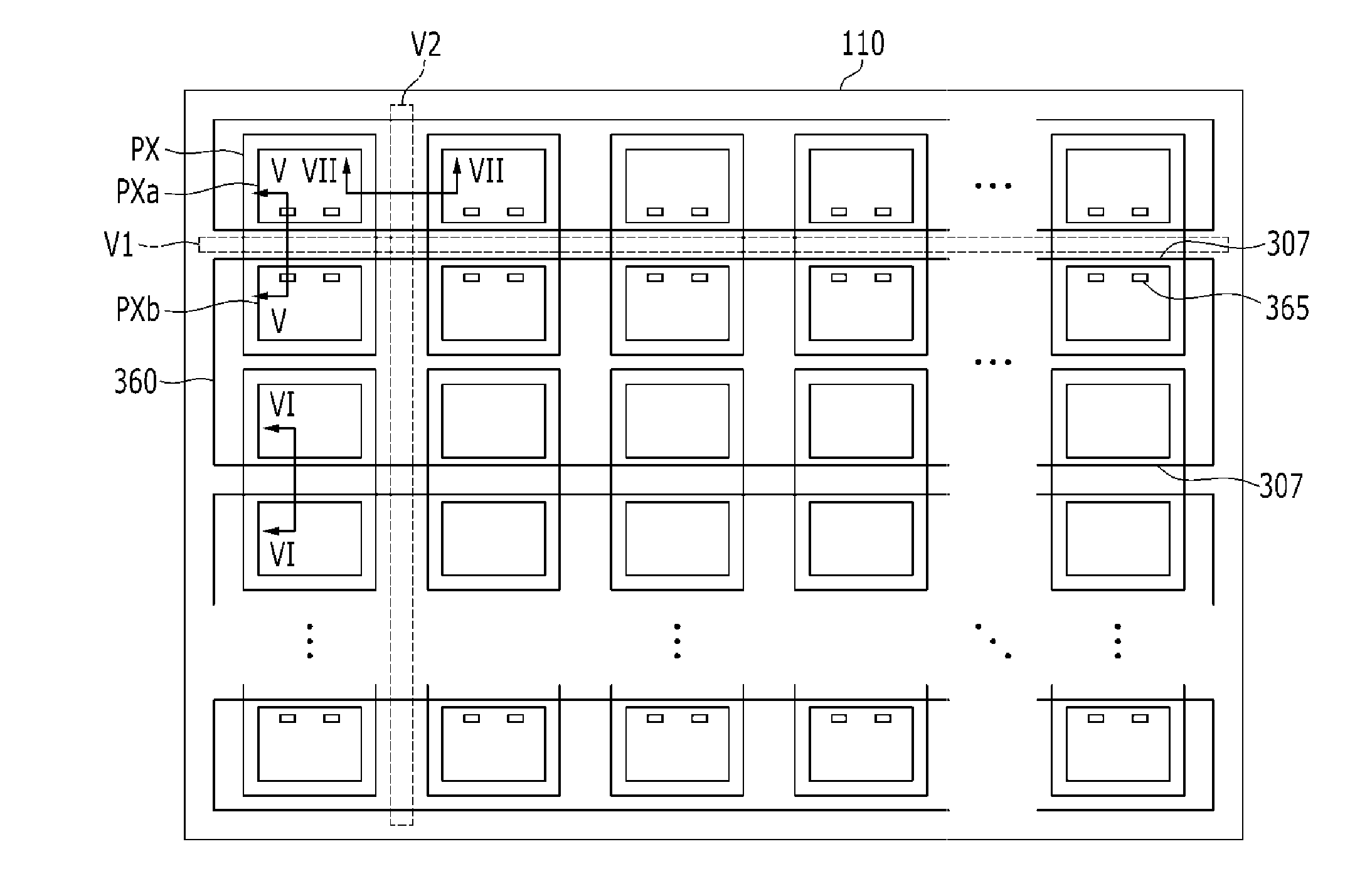
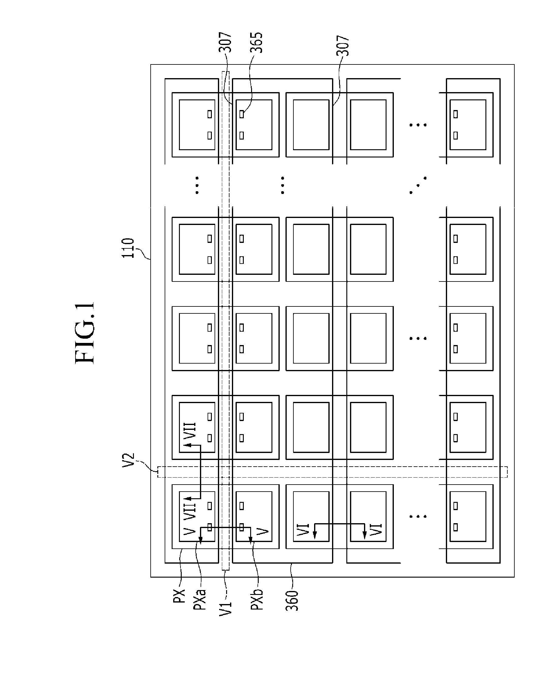
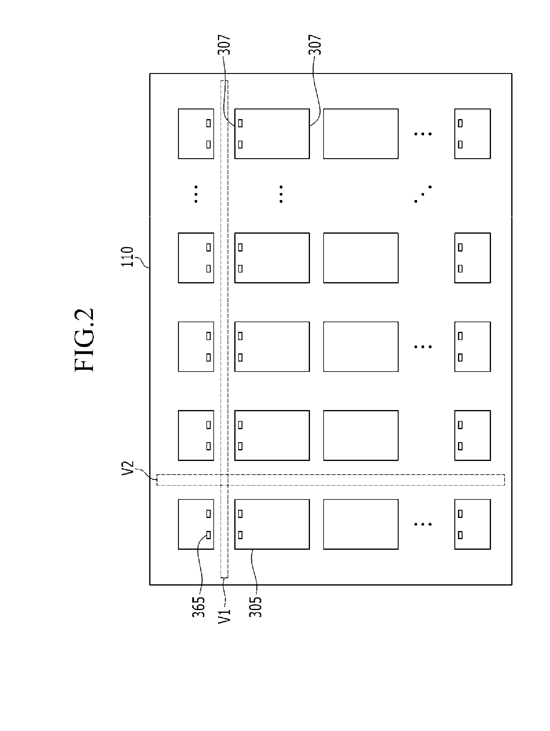
[0064]The present invention will be described more fully hereinafter with reference to the accompanying drawings, in which embodiments of the invention are shown. As those skilled in the art would realize, the described embodiments may be modified in various different ways, all without departing from the spirit or scope of the present invention.

[0065]In the drawings, the thicknesses of layers, films, panels, regions, etc., may be exaggerated for clarity. Like reference numerals may designate like elements in the specification. If an element such as a layer, film, region, or substrate is referred to as being “on” another element, it can be directly on the other element, or at least one intervening element may also be present. In contrast, if an element is referred to as being “directly on” another element, there are no intended intervening elements (except one or more environmental elements, such as air) present.

[0066]Although the terms first, second, etc. may be used herein to descr...


PUM


Abstract

A display device may include a first subpixel electrode; a first roof layer; a first liquid crystal layer disposed between the first subpixel electrode and the first roof layer; and a first support member overlapping a first end portion of the first roof layer in a first direction. The display device may further include a second subpixel electrode immediately neighboring the first subpixel electrode; a second roof layer; a second liquid crystal layer disposed between the second subpixel electrode and the second roof layer; and a second support member overlapping a first end portion of the second roof layer in the first direction. The first end portion of the first roof layer and the first end portion of the second roof layer may be disposed between a second end portion of the first roof layer and a second end portion of the second roof layer.

Description

CROSS-REFERENCE TO RELATED APPLICATION[0001]This application claims priority to and the benefit of Korean Patent Application No. 10-2013-0063042 filed in the Korean Intellectual Property Office on May 31, 2013, the entire contents of which are incorporated herein by reference.BACKGROUND[0002](a) Technical Field[0003]The present invention relates to a display device and a manufacturing method thereof.[0004](b) Description of the Related Art[0005]A liquid crystal display typically includes two field generating electrodes, such as a pixel electrode and a common electrode, and a liquid crystal layer interposed therebetween. The field generating electrodes may generate an electric field in the liquid crystal layer to determine an orientation of liquid crystal molecules of the liquid crystal layer for controlling transmission of incident light, thereby displaying images.[0006]A conventional liquid crystal display typically requires a thin film transistor array panel and an opposite panel....

Claims


Application Information

Patent Timeline
IPC IPC(8): G02F1/1343
CPCG02F1/1343G02F1/1341G02F1/1333G02F1/1368G02F1/133308G02F1/133345G02F1/133377G02F1/1339G02F1/13392G02F1/134309G02F1/134345
Inventor LEE, SEON UKWON, SUNG HWANLEE, DAE HOLEE, SUN HWAJUNG, KWANG-CHUL
Owner SAMSUNG DISPLAY CO LTD
Why Eureka
Try Eureka