Semiconductor system and semiconductor package

a semiconductor and semiconductor technology, applied in the field of semiconductor systems, can solve the problems of data loss, large amount of current consumed, and large amount of current consumed, and achieve the effect of preventing excessive peak curren

Active Publication Date: 2014-12-04
SK HYNIX INC
View PDF5 Cites 15 Cited by
  • Summary
  • Abstract
  • Description
  • Claims
  • Application Information

AI Technical Summary

Benefits of technology

[0009]Various embodiments are directed to a technique for preventing the occurrence of excessi

Problems solved by technology

However, since the initial charge stored in the capacitor disappears due to leakage current caused by a PN junction of a MOS transistor or the like, the data may be lost.
Since data are rewritten to a large number of memory cells during the refresh operation, a large amount of c

Method used


Image

  • Semiconductor system and semiconductor package
  • Semiconductor system and semiconductor package
  • Semiconductor system and semiconductor package

Examples


Embodiment Construction

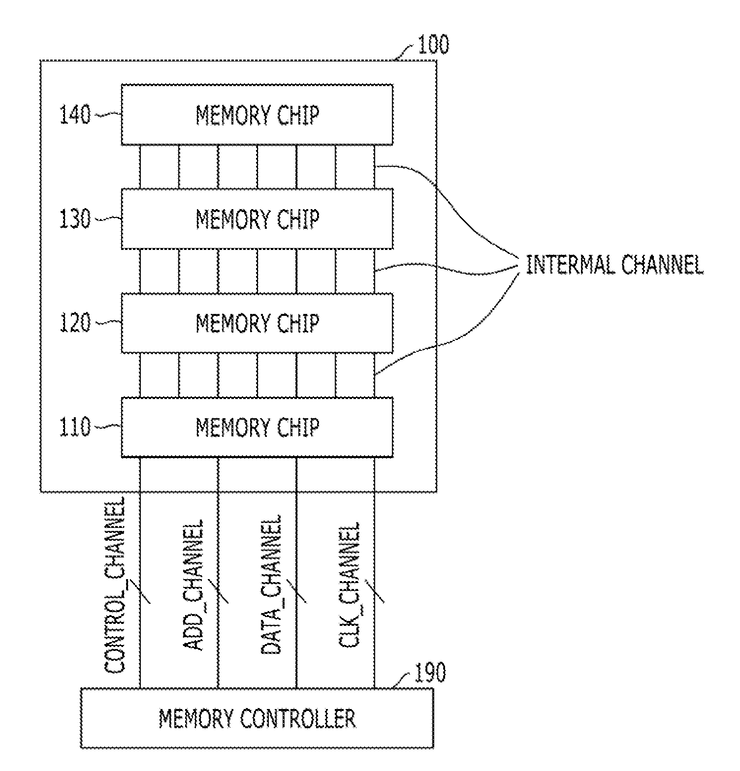
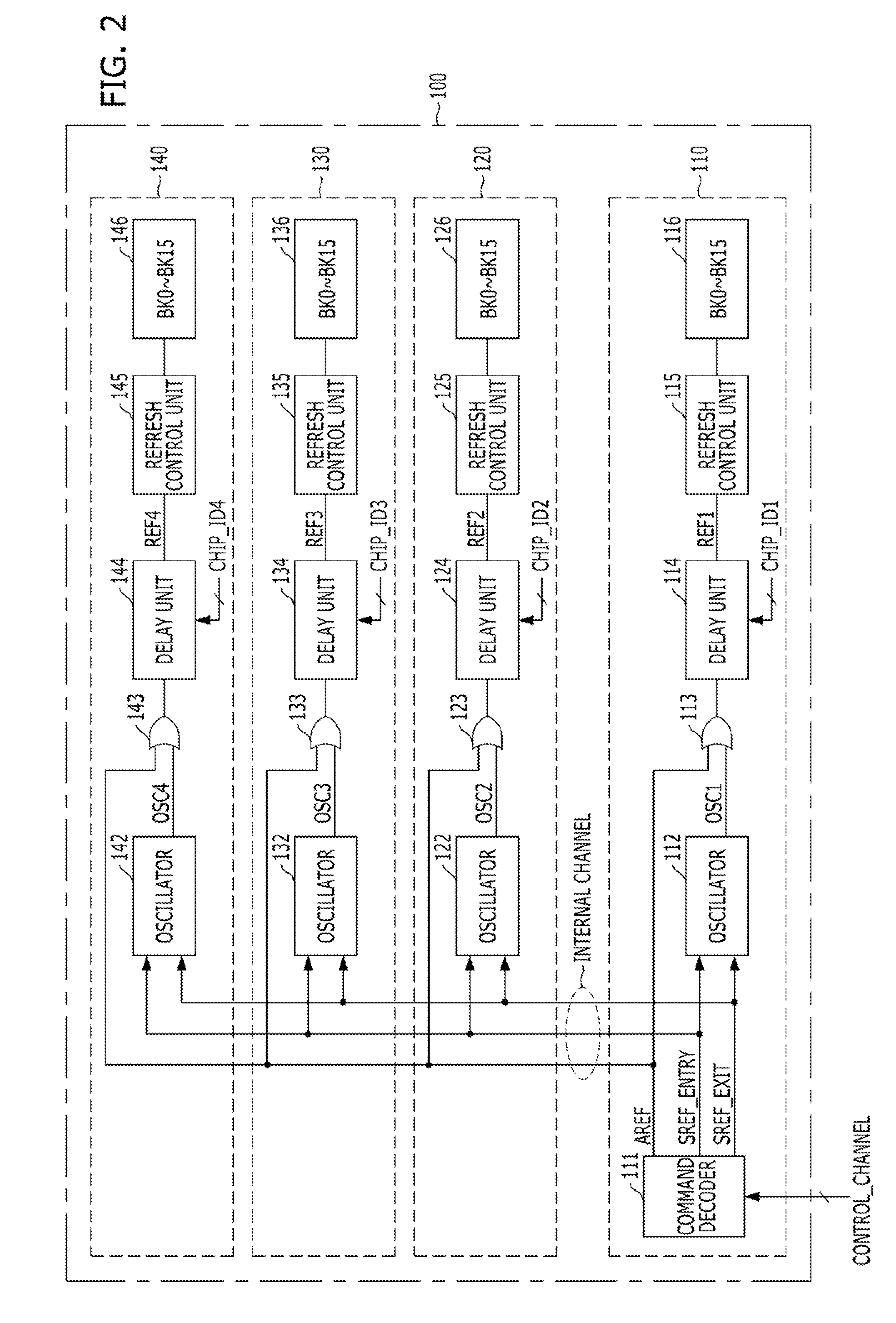
[0022]Various embodiments will be described below in more detail with reference to the accompanying drawings. The present invention may, however, be embodied in different forms and should not be construed as limited to the embodiments set forth herein. Rather, these embodiments are provided so that this disclosure will be thorough and complete, and will fully convey the scope of the present invention to those skilled in the art. Throughout the disclosure, reference numerals correspond directly to the like numbered parts in the various figures and embodiments of the present invention. It should be readily understood that the meaning of “on” and “over” in the present disclosure should be interpreted in the broadest manner such that “on” means not only “directly on” but also “on” something with an intermediate feature(s) or a layer(s) therebetween, and that “over” means not only directly on top but also on top of something with an intermediate feature(s) or a layer(s) therebetween. It ...


PUM


Abstract

A semiconductor system includes a plurality of memory chips. Each of the memory chips includes an oscillator suitable for generating a periodic wave in a self refresh mode, and a delay unit suitable for delaying the periodic wave to generate a refresh pulse and for setting a delay value based on a corresponding chip identification.

Description

CROSS-REFERENCE TO RELATED APPLICATIONS[0001]The present application claims priority of Korean Patent Application No 10-2013-0060309, filed on May 28, 2013, which is incorporated herein by reference in its entirety.BACKGROUND[0002]1. Field[0003]Exemplary embodiments of the present invention relate to a semiconductor system, and more particularly, to a technology for refreshing stored data.[0004]2. Description of the Related Art[0005]A memory cell within a volatile memory device, such as a DRAM, includes a transistor serving as an access element and a capacitor serving as a storage element. According to whether or not a charge is stored in the capacitor of the memory cell, that is, according to whether the terminal voltage of the capacitor is high or low, data is divided into ‘high’ (logic 1) and ‘low’ (logic 0).[0006]Since data are retained in such a form that charges are accumulated, no power is theoretically consumed. However, since the initial charge stored in the capacitor disap...

Claims


Application Information

Patent Timeline
IPC IPC(8): G11C5/00
CPCG11C5/005G11C11/40615G11C11/40618G11C29/023G11C29/028G11C2029/4402G11C2211/4067G11C11/402G11C11/406
Inventor KIM, JUNG-HYUN
Owner SK HYNIX INC
Why Eureka
Try Eureka