Lc snubber circuit

a snubber circuit and circuit technology, applied in the direction of electric variable regulation, process and machine control, instruments, etc., can solve the problems of large voltage/current stress on the switch q and the diode dsub>o, large power loss, and limited voltage stress margin of the switching device in the switching converter, so as to reduce the circulating current

Inactive Publication Date: 2014-12-11
ABB RES LTD
View PDF3 Cites 13 Cited by
  • Summary
  • Abstract
  • Description
  • Claims
  • Application Information

AI Technical Summary

Benefits of technology

[0008]A method is also disclosed for a switching converter having a first converter inductor connected between a first connection node and a second connection node, and a first converter switching device connected between the second connection node and a third connection node, wherein the method comprises: using an LC snubber for limiting a maximum voltage stress of the first converter switching device; and transferring energy stored in the LC snubber to an output through a snubber transformer coupled with the output in order to reduce circulating currents in the LC snubber.

Problems solved by technology

An RCD snubber is widely used in cost-sensitive applications, but it may cause rather large power losses.
At the cost of the simple structure, however, the flyback may suffer from a large voltage / current stress on the switch Q and the diode Do.
The voltage stress margin of the switching device in the switching converter may be very limited in some high supply voltage applications, such as a three-phase auxiliary power supply (APS), where the supply voltage may reach 1200 V. Thus, the snubber may have to be able to limit additional voltage stress to a small range.
These circulating currents may induce additional conduction losses in the switch and in the snubber circuit itself.

Method used


Image

  • Lc snubber circuit
  • Lc snubber circuit
  • Lc snubber circuit

Examples


Embodiment Construction

[0019]A method and an apparatus are disclosed for implementing the method so as to alleviate disadvantages discussed herein.

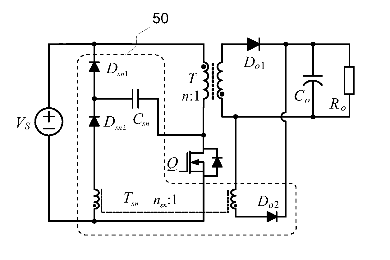
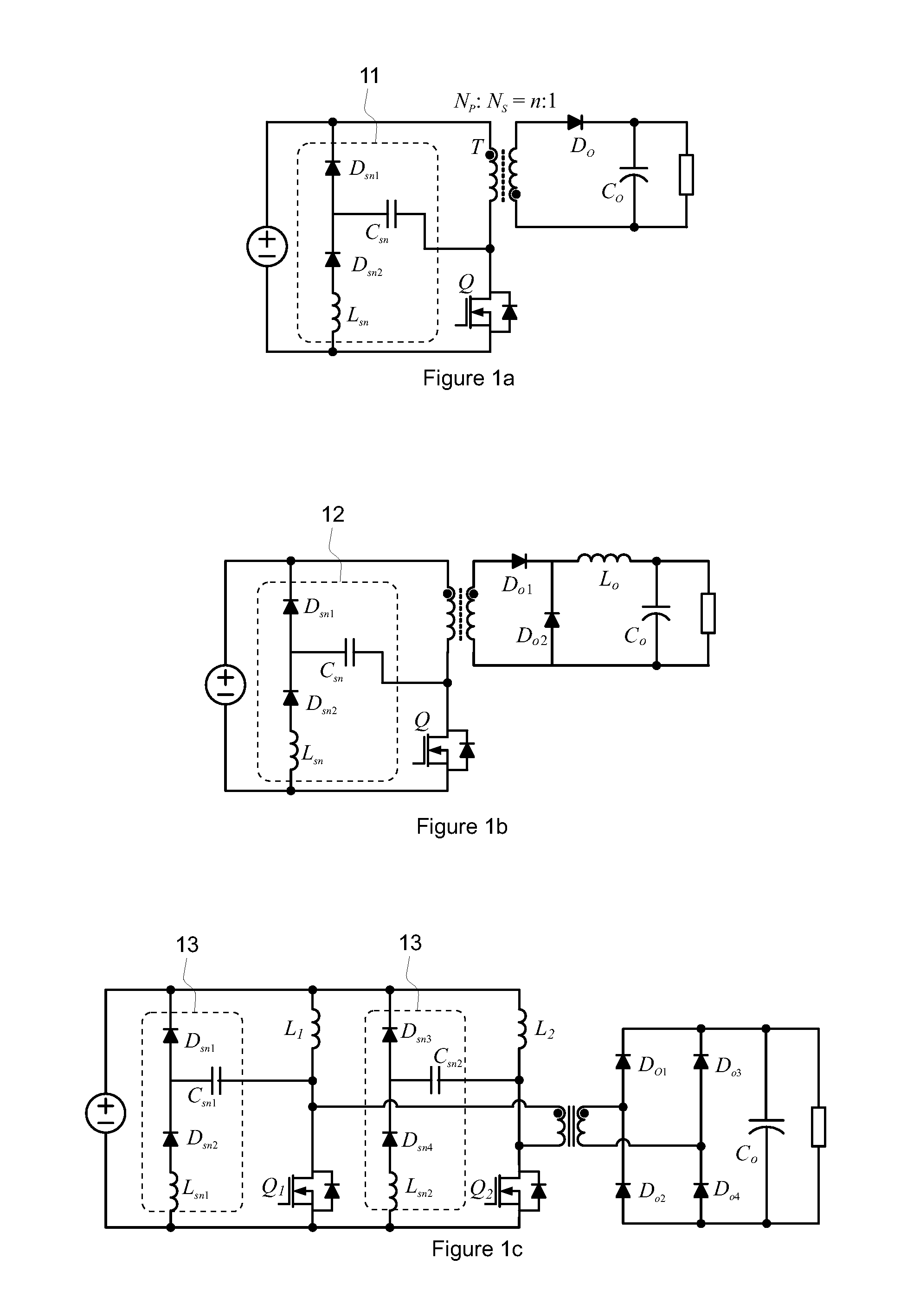
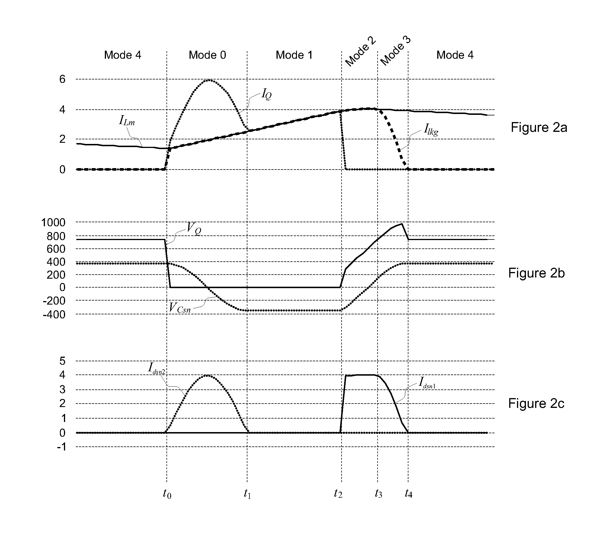
[0020]The present disclosure presents an enhanced LC snubber topology for a switching converter. The enhanced LC snubber can reduce circulating current compared with known LC snubbers. The proposed snubber has a coupling to the output of the switching converter through which energy stored in the snubber can be transferred to the output, which can minimise the circulating currents. This may lead to higher efficiency. The coupling to the output may be implemented by a transformer having its primary winding operating as the snubber inductance.

[0021]The disclosed LC snubber can provide an effective voltage clamping for the switch(es) of the switching converter. The peak voltage stress for the switch(es) can be reduced. This leads to lower switch voltage stress and higher reliability. The effective voltage clamping may also provide room for increased duty ratio, the...


PUM


Abstract

The present disclosure relates to an LC snubber circuit for a switching converter, wherein the switching converter includes an inductor and a switching device connected in series. The LC snubber circuit can include a first snubber diode, a snubber capacitor, a second snubber diode, and a snubber transformer having a primary winding and a secondary winding. The secondary winding of the snubber transformer is connected to an output of the switching converter.

Description

RELATED APPLICATION[0001]This application claims priority under 35 U.S.C. §119 to European Patent Application No. 13171354.7 filed in Europe on Jun. 11, 2013, the entire content of which is hereby incorporated by reference in its entirety.FIELD[0002]The present disclosure relates to LC snubber circuits, and for example to minimising circulating currents in an LC snubber circuit.BACKGROUND INFORMATION[0003]A variety of voltage snubber circuits have been developed for guaranteeing a voltage stress margin of semiconductors in switching converters. An RCD snubber is widely used in cost-sensitive applications, but it may cause rather large power losses. See, for example, [1] H.-S. Choi, “AN4137—Design guidelines for off-line flyback converters using Fairchild Power Switch (FPS)”, Fairchild Semiconductor Cor., 2003; and [2] S. Buonomo, F. Saya, and G. Vitale, “AN1889—STCO3DE170 in 3-phase auxiliary power supply,” STMicroelectronics, 2003.[0004]An LC snubber may provide an alternative solu...

Claims


Application Information

Patent Timeline
Patent Type & Authority Applications(United States)
IPC IPC(8): H02M1/34H02M3/335
CPCH02M1/34H02M2001/346H02M3/33523H02M3/335H02M1/346Y02B70/10
Inventor PARK, KI-BUMCANALES, FRANCISCOPETTERSSON, SAMI
Owner ABB RES LTD
Why Eureka
Try Eureka