
Semiconductor device having level shift circuit

a technology of level shift circuit and semiconductor device, which is applied in the direction of digital storage, pulse automatic control, instruments, etc., can solve the problems of leakage current and decrease of the effective width (window width) of read data

Active Publication Date: 2015-01-01
MICRON TECH INC
View PDF11 Cites 9 Cited by
  • Summary
  • Abstract
  • Description
  • Claims
  • Application Information

AI Technical Summary

Benefits of technology

The patent describes a semiconductor device including a level conversion circuit and a delay circuit that work together to produce an output signal with a controlled amplitude. The device also includes first and second transistors that are controlled by the second and third signals, respectively. The technical effect of this invention is to provide a more precise and controlled output signal for better performance and reliability of the semiconductor device.

Problems solved by technology

This causes a leak current.
Therefore, a problem arises, for example, in that the effective width (window width) of read data is decreased,

Method used


Image

  • Semiconductor device having level shift circuit
  • Semiconductor device having level shift circuit
  • Semiconductor device having level shift circuit

Examples


first embodiment

[0053]Turning to FIG. 4, the level shift circuit 100B is different from the level shift circuit 100A shown in FIG. 3 in that the inverter circuit 140 is replaced with an output circuit 140B, and an inverter circuit 150 is added. Other features of the level shift circuit 100B are basically identical to those of the level shift circuit 100A shown in FIG. 3, and thus like reference numerals are denoted to like elements and redundant explanations thereof will be omitted.

[0054]The inverter circuit 150 is constituted by a P-channel MOS transistor MP3 and an N-channel MOS transistor MN3 that are connected in series between a power supply line, to which the internal power-supply potential VPERI is supplied, and a power supply line, to which the ground potential VSS is supplied. An input node of the inverter circuit 150 is connected to the node T2A. An output node of the inverter circuit 150 is connected to a node T3A.

[0055]The output circuit 140B is constituted by the P-channel MOS transis...

second embodiment

[0065]the present invention is explained next.

[0066]Turning to FIG. 5, the level shift circuit 100C according to the second embodiment is different from the level shift circuit 100B shown in FIG. 4 in that the output circuit 140B is replaced with an output circuit 140C. Other features of the level shift circuit. 100C are basically identical to those of the level shift, circuit 100B shown in FIG. 4, and thus like reference numerals are denoted to like elements and redundant explanations thereof will be omitted.

[0067]The output circuit 140C has a configuration in which the transistor MN22 is connected in parallel to the transistor MN21 included in the inverter circuit 140 shown in FIG. 3. That is, the output circuit 140C has a circuit configuration in which the inverter circuit 140 shown in FIG. 3 and the output circuit 140B shown in FIG. 4 are combined. However, it is preferable to set the current drive capabilities of the transistors MN21 and MN22 to be smaller than the current driv...

third embodiment

[0072]the present invention is explained next.

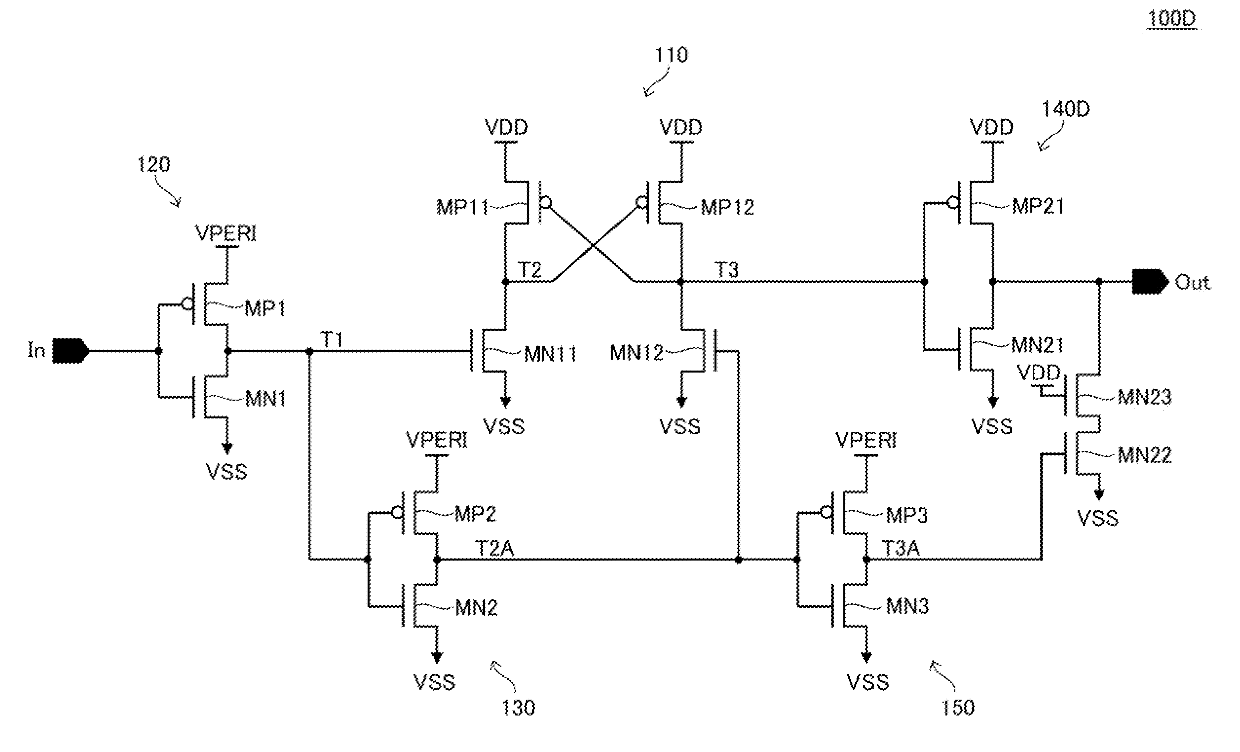
[0073]Turning to FIG. 7, the level shift circuit 100D according to the third embodiment is different from the level shift circuit. 100C shown in FIG. 5 in that the output circuit 140C is replaced with an output circuit 140D. Other features of the level shift circuit 100D are basically identical to those of the level shift circuit 100C shown in FIG. 5, and thus like reference numerals are denoted to like elements and redundant explanations thereof will be omitted.

[0074]The output circuit 140D is different from the output circuit. 140C in that an N-channel MOS transistor MM23 that is connected in series to the transistor MN22 is added. The external power-supply potential VDD is supplied to a gate electrode of the transistor MN23 in a fixed manner. Therefore, the transistor MN23 is normally in the on state, however, its on-resistance is changed according to the level of the external power-supply potential VDD. Specifically, as the level of ...


PUM


Abstract

Disclosed herein is a device includes; a level conversion circuit coupled to first and third power supply lines, receiving a first signal and an inverted signal of the first signal each having an amplitude between first and second potentials, and output ting a second signal having an amplitude between first and third potentials; a delay circuit coupled to the first and second power supply lines, and output ting a third signal delayed from the first signal; and an output circuit including first and second transistors coupled in series between the first and third power supply lines, the first transistor having a control electrode supplied with the second signal, and the second transistor having a control electrode supplied with the third signal.

Description

BACKGROUND[0001]1. Field of the Invention[0002]Embodiments of the present invention relate to a semiconductor device, and more particularly relate to a semiconductor device including a level shift circuit that converts the voltage amplitude of a signal.[0003]2. Description of Related Art[0004]Some semiconductor devices include a level shift circuit that converts the amplitude of a signal. There are two types of the level shift circuit, one of which is designed to decrease the signal amplitude and the other is designed to increase the signal amplitude. Among the two types, the level shift circuit designed to decrease the signal amplitude can foe configured by a simple inverter circuit. This is because the amplitude of the input-signal is larger than the amplitude of the operating voltage of the inverter circuit, and therefore at either logic level of the input signal, one of the transistors that constitute the inverter circuit can be reliably switched to the off state.[0005]On the ot...

Claims


Application Information

Patent Timeline
Patent Type & Authority Applications(United States)
IPC IPC(8): H03K19/0185
CPCH03K19/0185G11C7/1039G11C5/147G11C7/106G11C7/1063G11C7/1066G11C7/1084G11C7/1087G11C7/1093G11C7/222G11C11/4074G11C11/4076G11C11/4093
Inventor NAKAMURA, KOHEI
Owner MICRON TECH INC
Learn More