
Flexible l-network antenna tuner circuit

a tuner circuit and flexible technology, applied in the field of impedance matching elements, can solve the problems of reducing the power transfer between the antenna and the amplifier circuit or the transceiver, affecting the impedance of the circuit elements, and sometimes inability to determine a priori,

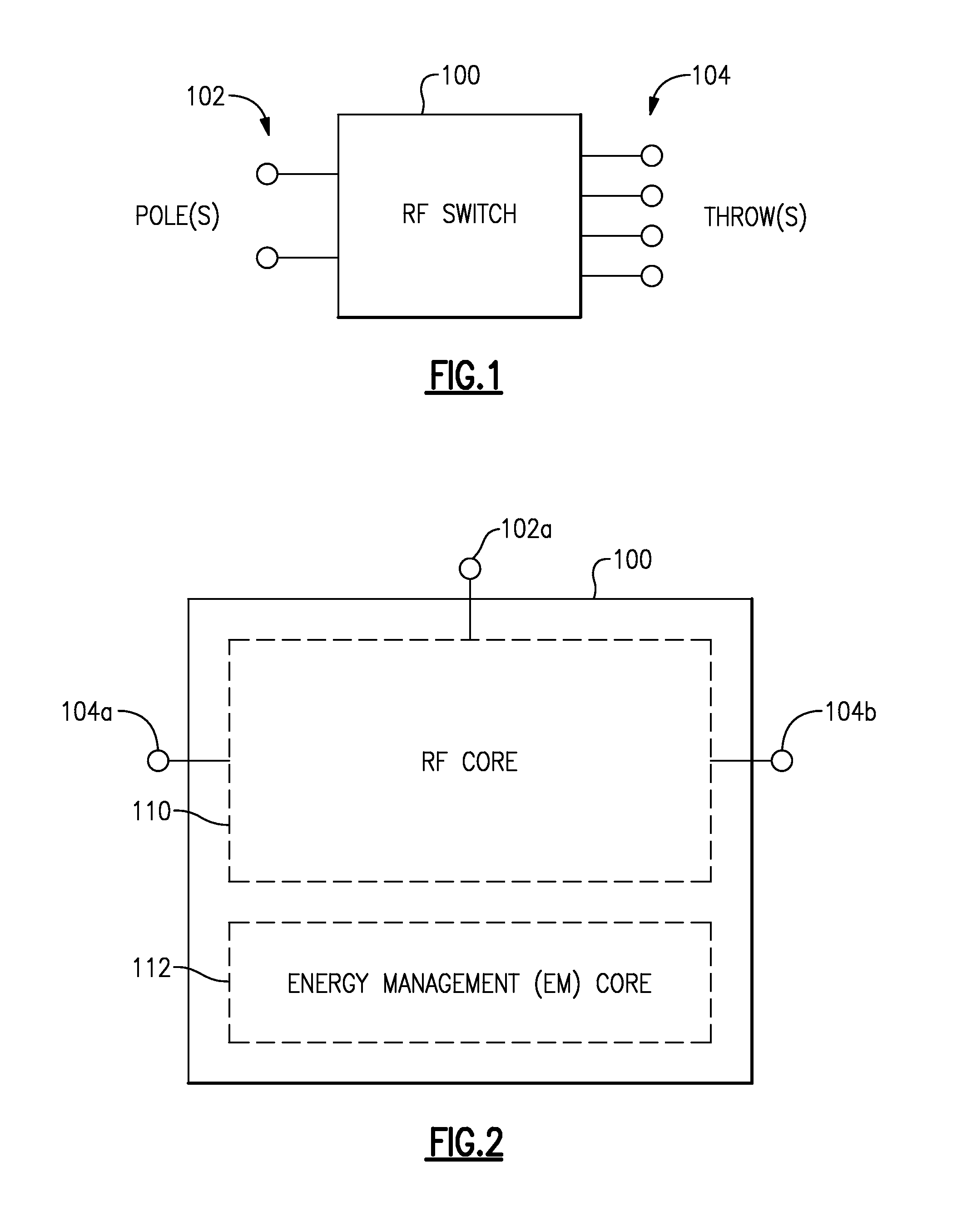
Active Publication Date: 2015-01-01
SKYWORKS SOLUTIONS INC
View PDF2 Cites 18 Cited by
  • Summary
  • Abstract
  • Description
  • Claims
  • Application Information

AI Technical Summary

Benefits of technology

The present disclosure relates to an impedance matching circuit that can be used in wireless devices. The circuit includes a series element and a shunt element that can be switched to different positions to match the impedance of different elements in the device. The circuit can be controlled by a controller or a sensor, and can be used to transmit signals between the different elements. The technical effect of the invention is to improve the impedance matching of different elements in a wireless device, which can enhance signal quality and reduce interference.

Problems solved by technology

Further, in some cases, environmental factors, such as the positioning of a device may affect the impedance for the circuit elements.
For example, a mismatch between the impedance of an antenna and an amplifier circuit or a transceiver may result in reduced power transfer between the antenna and the amplifier circuit or the transceiver.
However, in certain cases, it can be challenging and sometimes infeasible to determine a priori which shunt element to omit from the impedance matching circuit.
One reason it is difficult to determine a priori the shunt element to omit is that the impedance for one or more of the circuit elements to be matched by the impedance matching circuit may fluctuate.
Further, in some cases, the impedance of the other device element may also fluctuate.
In some embodiments, a switching device can include device components that introduce parasitic capacitance, inductance, resistance, or conductance into the device, contributing to increased switching device insertion loss.
Accordingly, second and third orders can be undesirable effects that are of particular interest.
Non linearity in RF systems can result in introduction of spurious signals into the system.
Spurious signals in the RF system can result in interference within the system and degrade the information transmitted by RF signals.
Non-linearity in system components, for example switching devices, can contribute to the introduction of spurious signals into the RF system, thereby contributing to degradation of overall RF system linearity and IMD performance.
However, in some embodiments, increased FET stack height can degrade the switching device insertion loss performance.
Further, other conditions of the wireless device may also result in impedance changes in the components of the wireless device.
The inclusion of extra capacitors and inductors can increase both the size and cost of the impedance matching circuit 1300.

Method used


Image

  • Flexible l-network antenna tuner circuit
  • Flexible l-network antenna tuner circuit
  • Flexible l-network antenna tuner circuit

Examples


example l -

Example L-Network with Bypass Modes

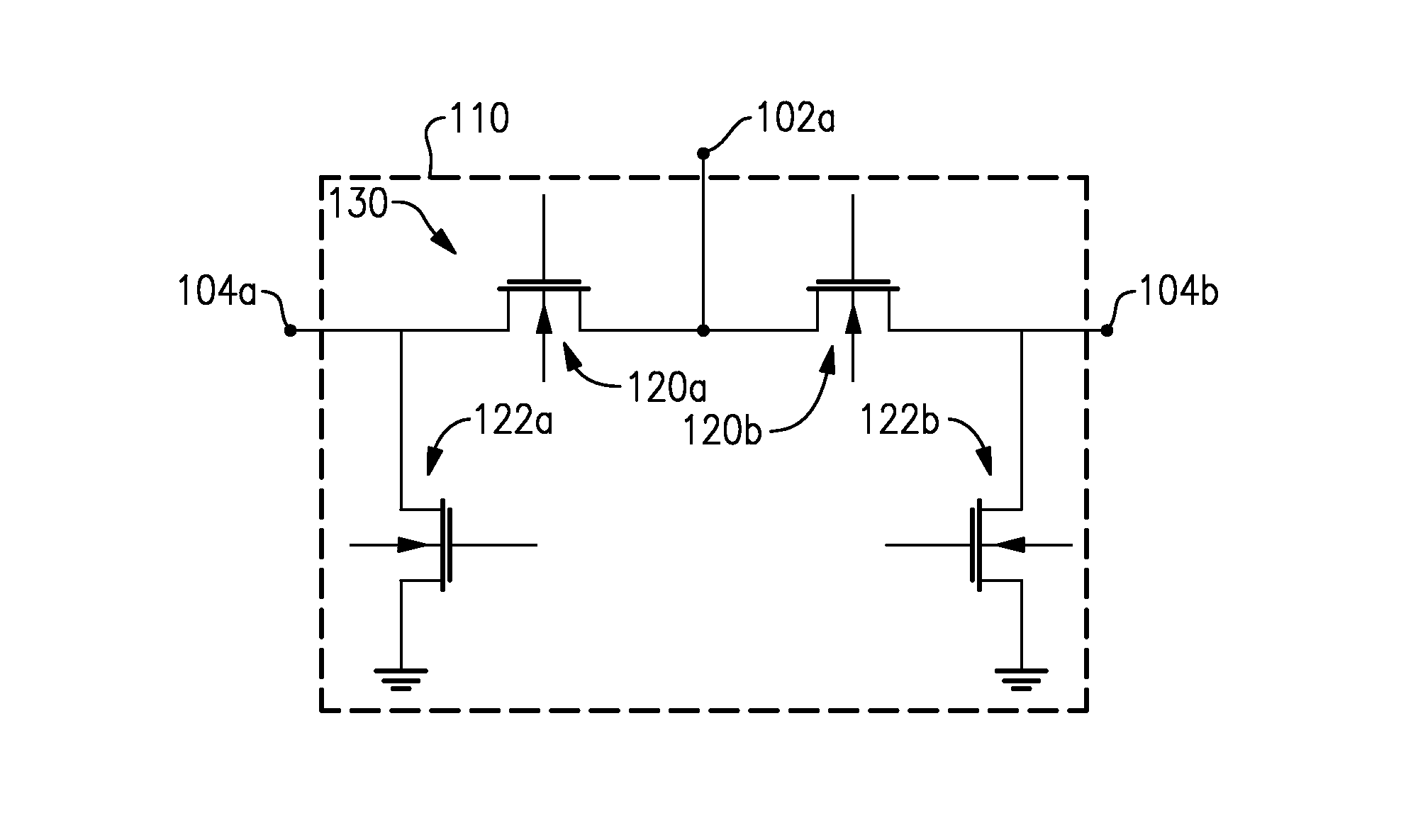
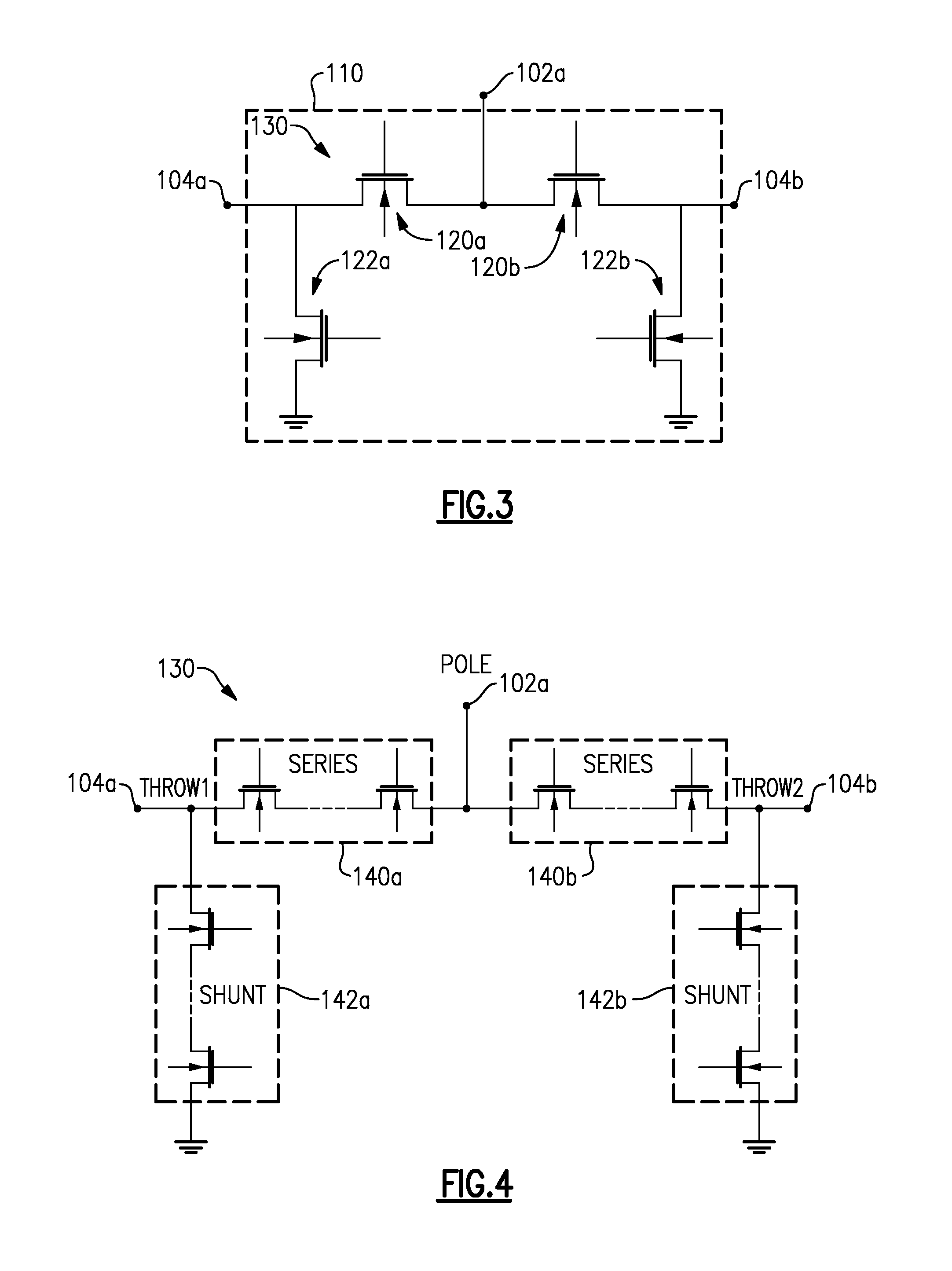
[0126]FIG. 21 illustrates an example of an L-network impedance matching circuit 2100 capable of bypass modes. In certain embodiments, the impedance matching circuit 2100 may include some or all of the embodiments described above with respect to the impedance matching circuits 1400 and 1800. Further, as with the impedance matching circuits 1400 and 1800, the impedance matching circuit 2100 may include a pair of nodes 2106 and 2108 for electrically communicating with circuits or devices of a wireless device, or otherwise, with impedances that may, at least in some cases, be mismatched. Further, as previously described with respect to the impedance matching circuits 1400 and 1800, the impedance matching circuit 2100 may include a capacitor C1 between the nodes 2106 and 2108, and a shunt circuit, which may include the capacitor C2 and the inductor L.

[0127]In addition, the impedance matching circuit 2100 may include a switch SW. As illustrated in FIG. 2...


PUM


Abstract

An ‘L’ shaped dynamically configurable impedance matching circuit is presented herein. The circuit can include a series element and a shunt element. The shunt element in the L-shaped impedance matching circuit can be moved or modified based on the impedance of the circuit elements in electrical communication with each side of the impedance matching circuit. Thus, in some cases, the impedance matching circuit may be a flexible circuit that can be dynamically modified based on the environment or configuration of the wireless device that includes the impedance matching circuit.

Description

RELATED APPLICATIONS[0001]This disclosure claims priority to U.S. Provisional Application No. 61 / 841,217 filed Jun. 28, 2013 and entitled “FLEXIBLE L-NETWORK ANTENNA TUNER CIRCUIT,” the disclosure of which is expressly incorporated by reference herein in its entirety.TECHNICAL FIELD[0002]The present disclosure relates generally to impedance matching elements. More specifically, the present disclosure relates to flexible and tunable impedance matching elements.BACKGROUND[0003]Radio Frequency (RF) switches, such as transistor switches, can be used to switch signals between one or more poles and one or more throws. Transistor switches, or portions thereof, can be controlled through transistor biasing and / or coupling. Design and use of bias and / or coupling circuits in connection with RF switches can affect switching performance.[0004]In some cases, circuit elements may generate different impedance values. To improve performance of a circuit, it is often desirable to select circuit eleme...

Claims


Application Information

Patent Timeline
Patent Type & Authority Applications(United States)
IPC IPC(8): H04L5/08H03H11/28
CPCH04L5/08H03H11/28
Inventor DOMINO, WILLIAM J.WLOCZYSIAK, STEPHANE RICHARD MARIE
Owner SKYWORKS SOLUTIONS INC
Learn More