Display device

a display device and display technology, applied in the field of display devices, can solve problems such as light loss

Active Publication Date: 2015-01-08
SAMSUNG DISPLAY CO LTD
View PDF4 Cites 41 Cited by
  • Summary
  • Abstract
  • Description
  • Claims
  • Application Information

AI Technical Summary

Benefits of technology

[0011]Still other aspects, features, and advantages of the present invention are readily apparent from the following detailed description, simply by illustrating a number of particular embodiments and implementations, including the best mode contemplated for carrying out the present invention. The present invention is also capable of other and different embodiments, and its several details can be modified in various obvious respects, all without departing from the spirit and scope of the present invention. Accordingly, the drawing and description are to be regarded as illustrative in nature, and not as restrictive.
[0012]Exemplary embodiments of the present invention disclose a display device. The display device includes a light source. The device includes a thin film transistor array panel including a pixel electrode and a common electrode. The device includes an upper panel. The device includes a quantum rod layer positioned between the thin film transistor array panel and the upper panel. The device includes a polarizer attached outside of the upper panel. The quantum rod layer includes quantum rods, and an arrangement direction of the quantum rods is controlled by an electric field generated by the pixel electrode and the common electrode, wherein light is polarized according to the controlled arrangement direction. The polarizer is

Problems solved by technology

In this general configuration, there is a light loss problem in a way of light emitted from a b

Method used


Image

  • Display device
  • Display device
  • Display device

Examples


Embodiment Construction

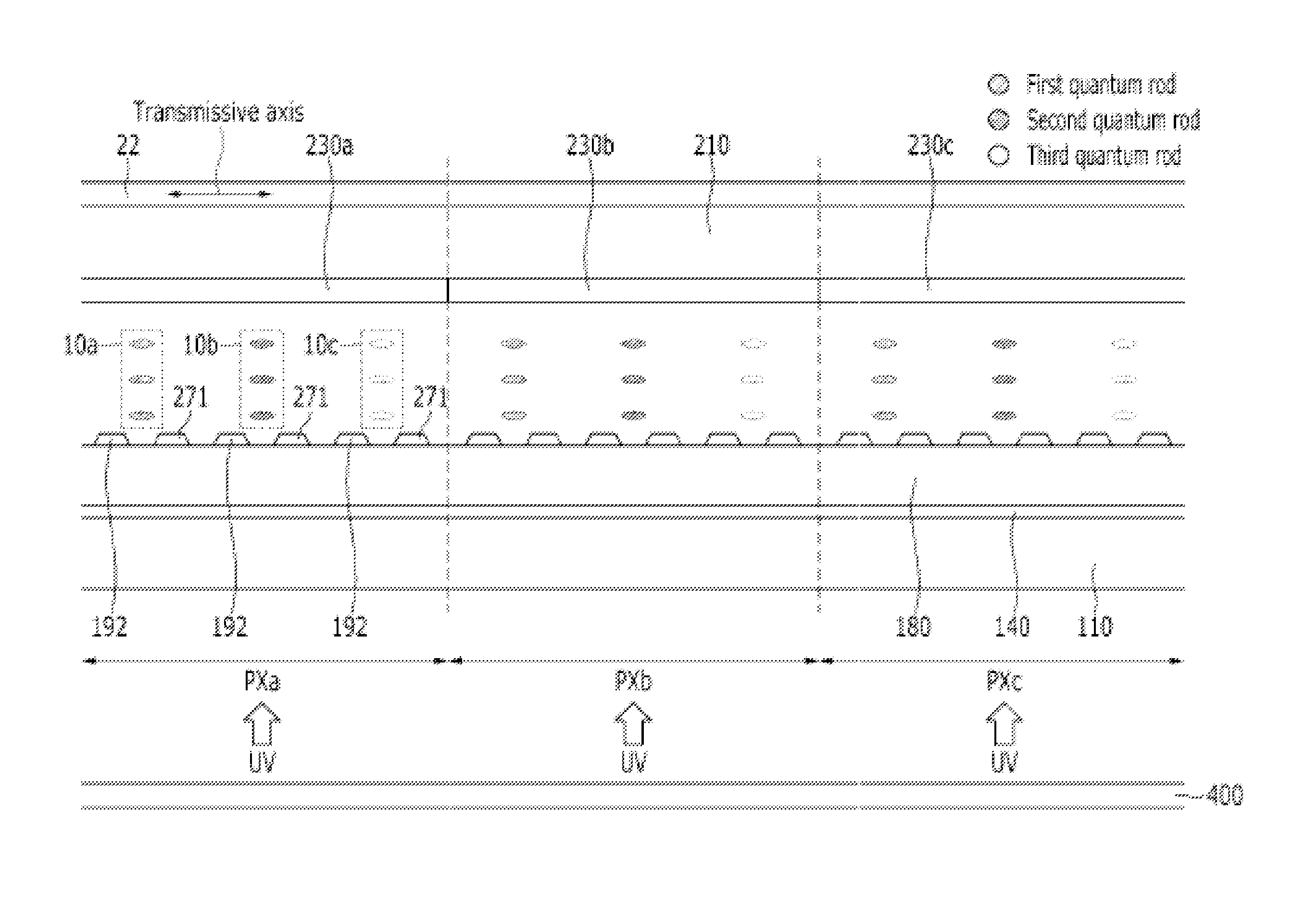
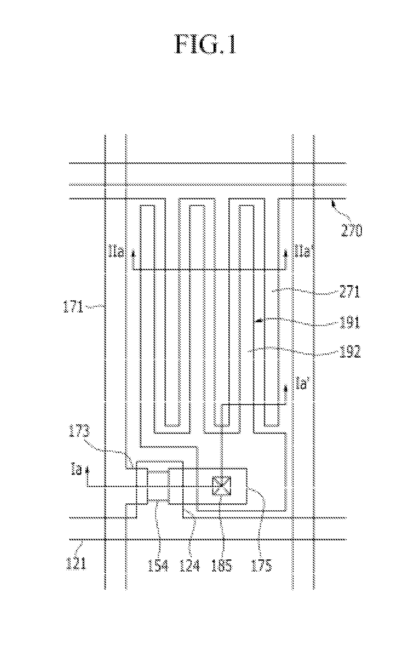
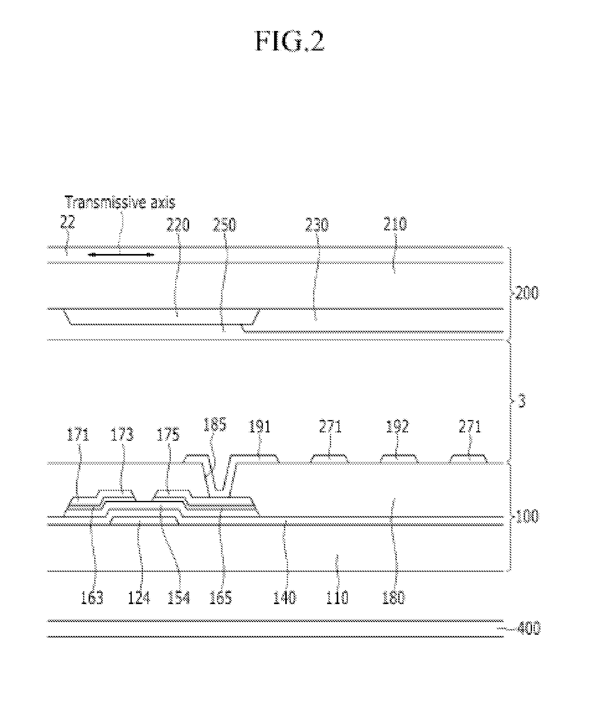
[0025]A display device and a method for manufacturing a display device using a quantum rod layer are disclosed. In the following description, for the purposes of explanation, numerous specific details are set forth in order to provide a thorough understanding of the present invention. It is apparent, however, to one skilled in the art that the present invention may be practiced without these specific details or with an equivalent arrangement. In other instances, well-known structures and devices are shown in block diagram form in order to avoid unnecessarily obscuring the present invention.

[0026]The present invention will be described more fully hereinafter with reference to the accompanying drawings, in which exemplary embodiments of the invention are shown. As those skilled in the art would realize, the described embodiments may be modified in various different ways, all without departing from the spirit or scope of the present invention.

[0027]In the drawings, the thickness of lay...


PUM


Abstract

A display device includes a light source generating light and a thin film transistor array panel including a pixel electrode and a common electrode. The display includes an upper panel and a quantum rod layer positioned between the thin film transistor array panel and the upper panel. The display includes an upper polarizer attached outside of the upper panel, in which the quantum rod layer includes quantum rods, and an arrangement direction of the quantum rods is controlled by an electric field generated by the pixel electrode and the common electrode, light is polarized according to the controlled arrangement direction, and the polarizer controls the transmission degree of the polarized light from the quantum rods according to the arrangement direction of the quantum rods.

Description

CROSS-REFERENCE TO RELATED APPLICATION[0001]This application claims priority to and the benefit of Korean Patent Application No. 10-2013-0077441, filed on Jul. 2, 2013, which is hereby incorporated by reference for all purposes as if fully set forth herein.BACKGROUND[0002]1. Field[0003]Exemplary embodiments of the present invention relate to a display device.[0004]2. Description of the Background[0005]Display devices have been developed from a cathode ray tube (CRT) using an existing cathode ray tube to various flat panel display devices such as a liquid crystal display (LCD), a plasma display panel (PDP), an organic light emitting display (OLED), an electrowetting display (EWD), an electrophoretic display (EPD), an embedded micro cavity display (EMD), and a nano crystal display (NCD).[0006]Since the liquid crystal display (LCD) among the flat panel displays has advantages such as a small size, a light weight, and low power consumption, it has gradually received attention as a repla...

Claims


Application Information

Patent Timeline
IPC IPC(8): G02F1/1335H01L27/12
CPCG02F1/133528G02F2001/133531H01L27/1262H01L27/1214G02F1/133617G02F2/02G02F2202/36G02B5/20G02B5/30
Inventor LEE, BAEK HEEKANG, JONG HYUKPARK, JAE BYUNGCHO, HYUN MINHONG, SUNG-JIN
Owner SAMSUNG DISPLAY CO LTD
Why Eureka
Try Eureka