Resin sheet attaching method
- Summary
- Abstract
- Description
- Claims
- Application Information
AI Technical Summary
Benefits of technology
Problems solved by technology
Method used
Image

Examples
Embodiment Construction
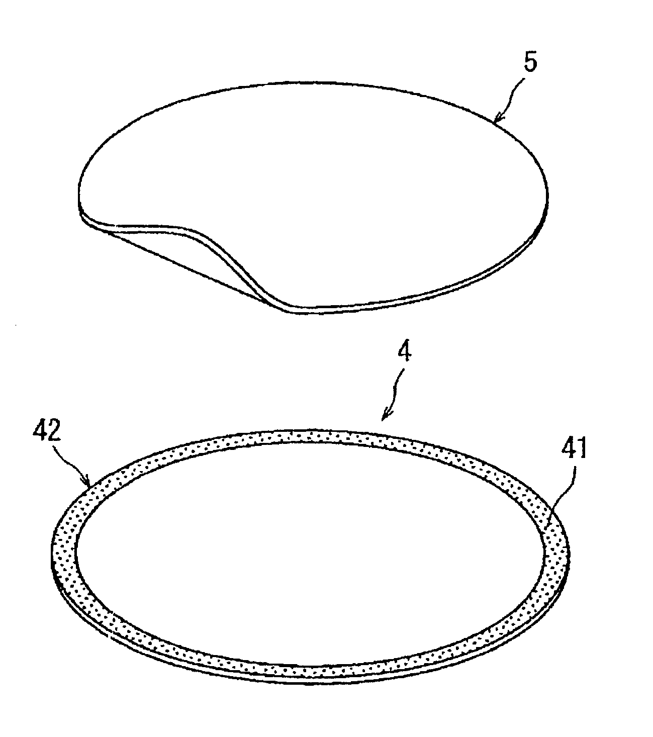
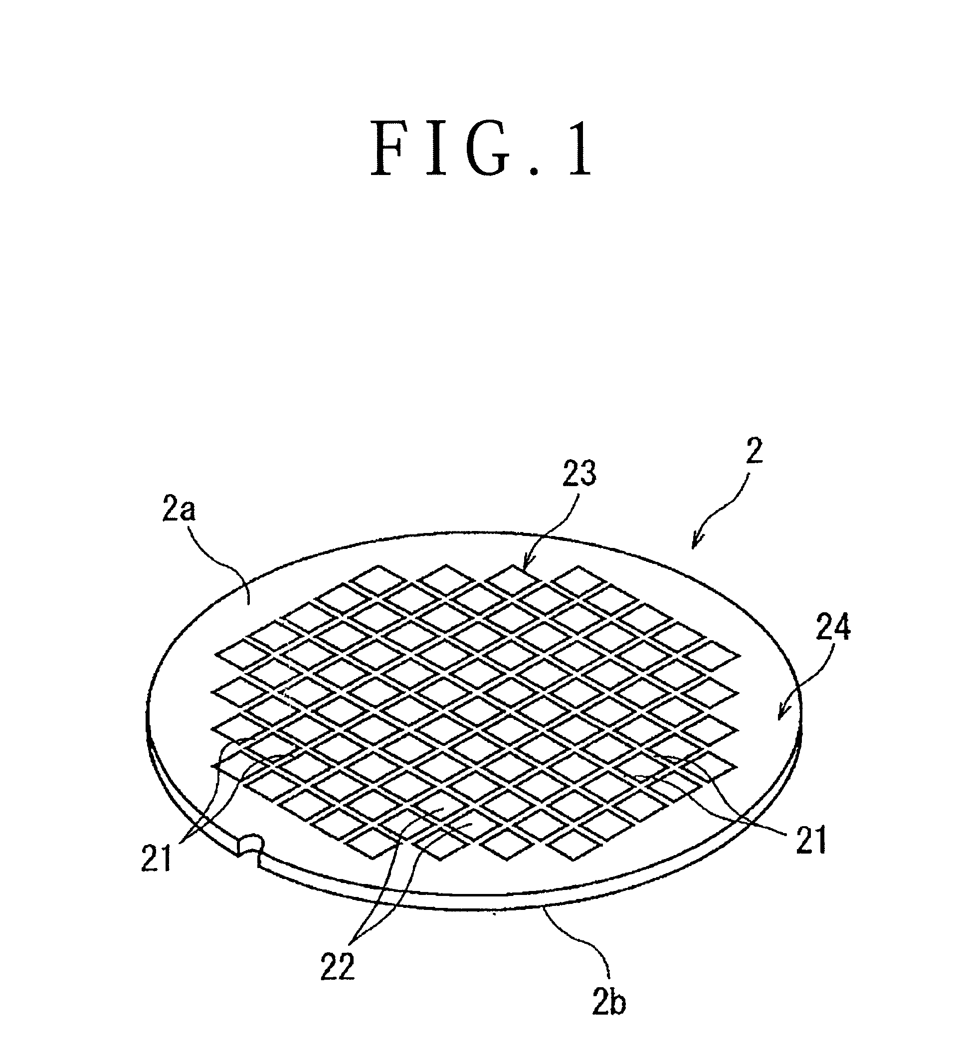
[0024]A preferred embodiment of the resin sheet attaching method according to the present invention will now be described in detail with reference to the attached drawings. FIG. 1 is a perspective view of a semiconductor wafer 2 as a workpiece. The semiconductor wafer 2 shown in FIG. 1 is a circular silicon wafer, which has a front side 2a and a back side 2b. A plurality of crossing division lines 21 are formed on the front side 2a of the semiconductor wafer 2 to thereby define a plurality of separate regions where a plurality of devices 22 such as ICs and LSIs are respectively formed. The front side 2a of the semiconductor wafer 2 includes a device area 23 where the devices 22 are formed and a peripheral marginal area 24 surrounding the device area 23. There will now be described a method of attaching a resin sheet to the front side 2a or the back side 2b of the semiconductor wafer 2.
[0025]More specifically, there will now be described a method of attaching a resin sheet to the fro...
PUM
| Property | Measurement | Unit |
|---|---|---|
| Nanoscale particle size | aaaaa | aaaaa |
| Force | aaaaa | aaaaa |
| Molecular weight | aaaaa | aaaaa |
Abstract
Description
Claims
Application Information
PatSnap Eureka turns technology decisions into work you can execute. Powered by our Innovation Knowledge Graph, it runs expert workflows across engineering, life sciences, materials and intellectual property. Get your review-ready output in minutes.


