Light emitting diode structure

a technology of light-emitting diodes and diodes, which is applied in the direction of semiconductor devices, basic electric elements, electrical apparatus, etc., can solve the problems of unsatisfactory light-emitting efficiency and the need to solve the problem of efficiently increasing the light-emitting efficiency of light-emitting diodes, and achieve excellent light-emitting efficiency

Active Publication Date: 2015-01-22
GENESIS PHOTONICS
View PDF14 Cites 9 Cited by
  • Summary
  • Abstract
  • Description
  • Claims
  • Application Information

AI Technical Summary

Benefits of technology

[0007]The invention provides a light emitting diode structure, which has excellent light-emitting efficiency.
[0023]In light of the foregoing, since the light emitting diode structure of the invention has a reflective conductive structure layer, and the reflective conductive structure layer covers a part of the semiconductor epitaxial layer and a portion of the substrate exposed by the semiconductor epitaxial layer, the reflective conductive structure layer is capable of effectively reflecting lights from the semiconductor epitaxial layer, and the portion of the substrate exposed by the semiconductor epitaxial layer also has reflecting effects. Thus, an arrangement of the reflective conductive structure layer can effectively enlarge reflective areas and can further effectively increase light-emitting efficiency of the light emitting diode structure as a whole.

Problems solved by technology

Although the aforesaid method can increase light-emitting efficiency of a light emitting diode, the light-emitting efficiency is no longer up to par.
Therefore, how to efficiently increase light-emitting efficiency of a light emitting diode is an issue required to be solved.

Method used


Image

  • Light emitting diode structure
  • Light emitting diode structure
  • Light emitting diode structure

Examples


Embodiment Construction

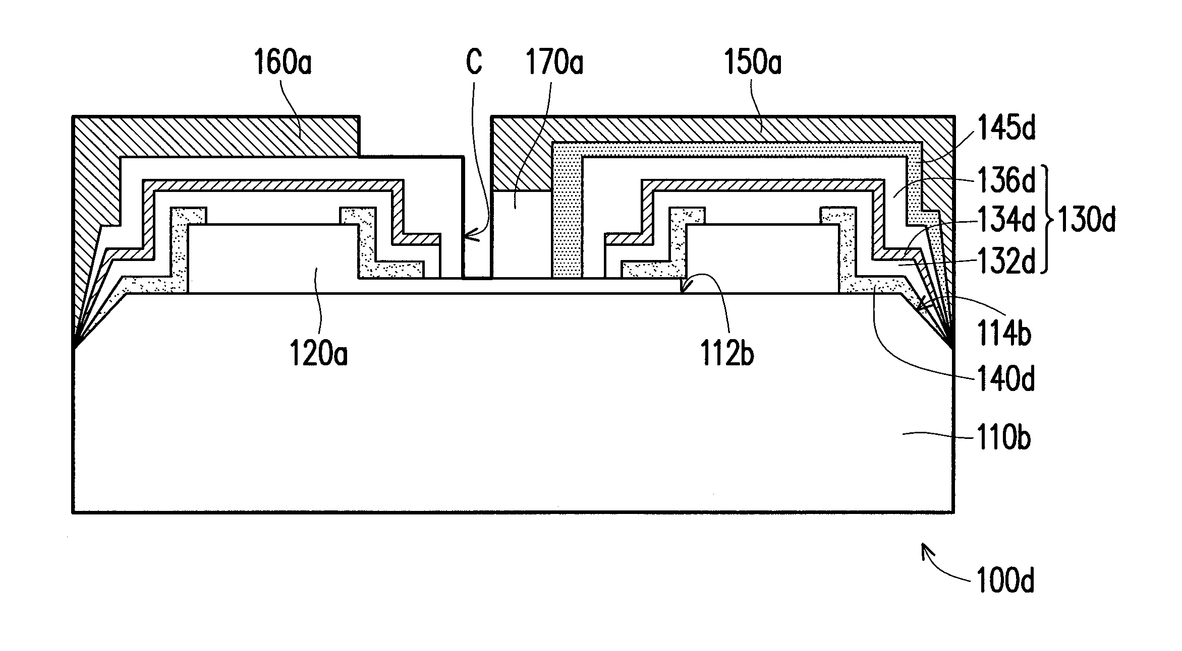
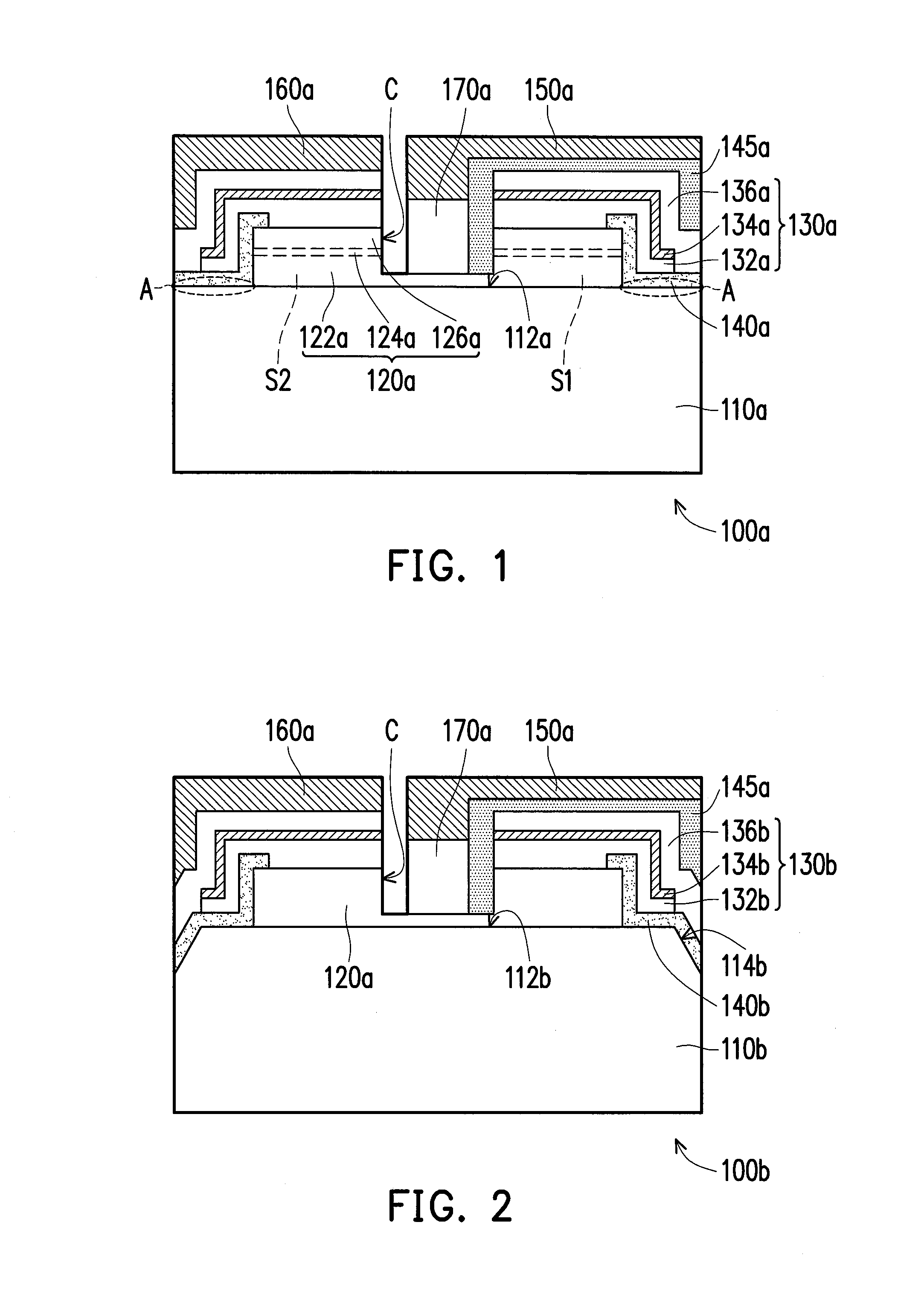
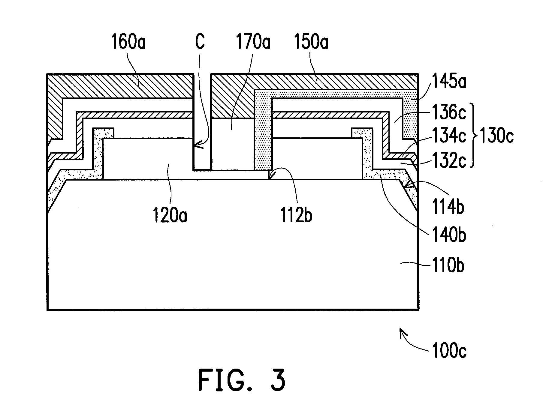
[0030]FIG. 1 is a cross-sectional view illustrating a light emitting diode structure according to an embodiment of the invention. Referring to FIG. 1, in the present embodiment, a light emitting diode structure 100a includes a substrate 110a, a semiconductor epitaxial layer 120a and a reflective conductive structure layer 130a. The semiconductor epitaxial layer 120a is disposed on the substrate 110a, and exposes a portion of the substrate 110a (dotted circular lines A as shown in FIG. 1). The reflective conductive structure layer 130a is disposed on the semiconductor epitaxial layer 120a, wherein the reflective conductive structure layer 130a covers a part of the semiconductor epitaxial layer 120a and the portion of the substrate 110a exposed by the semiconductor epitaxial layer 120a.

[0031]More specifically, in the present embodiment, the substrate 110a, for example, is a sapphire substrate. However, the invention is not limited thereto. The substrate 110a has an upper surface 112a...


PUM


Abstract

A light emitting diode structure including a substrate, a semiconductor epitaxial layer and a reflective conductive structure layer is provided. The semiconductor epitaxial layer is disposed on the substrate and exposes a portion of the substrate. The reflective conductive structure layer covers a part of the semiconductor epitaxial layer and the portion of the substrate exposed by the semiconductor epitaxial layer.

Description

CROSS-REFERENCE TO RELATED APPLICATION[0001]This application claims the priority benefit of Taiwan application serial no. 102125578, filed on Jul. 17, 2013. The entirety of the above-mentioned patent application is hereby incorporated by reference herein and made a part of this specification.BACKGROUND OF THE INVENTION[0002]1. Field of the Invention[0003]The invention relates to a semiconductor structure. More particularly, the invention relates to a light emitting diode structure.[0004]2. Description of Related Art[0005]Generally speaking, when fabricating a light emitting diode wafer, a substrate is usually provided first for an epitaxial structure to be formed on the substrate by using a method of an epitaxial growth. Then, electrodes are arranged on the epitaxial structure to provide electric energy, so as to emitting lights by using photoelectric effects. After that, pluralities of interlacing scribe lines are formed in the epitaxial structure via photolithographic and etching ...

Claims


Application Information

Patent Timeline
Patent Type & Authority Applications(United States)
IPC IPC(8): H01L33/40
CPCH01L33/405H01L33/42H01L33/36H01L33/38
Inventor HUANG, YI-RULO, YU-YUNWU, CHIH-LINGHUANG, JING-ENTING, SHAO-YING
Owner GENESIS PHOTONICS
Why Eureka
Try Eureka