Light emitting diode chip

a technology of light-emitting diodes and led chips, which is applied in the direction of electrical equipment, semiconductor devices, printing, etc., can solve the problems of less power used, longer battery life, and loss of absorption

Active Publication Date: 2015-01-29
META PLATFORMS TECH LLC
View PDF7 Cites 2 Cited by
  • Summary
  • Abstract
  • Description
  • Claims
  • Application Information

AI Technical Summary

Benefits of technology

[0038]According to the present disclosure in a third aspect, there is provided a method of manufacturing an LED chip. The method comprises fabricating an array of LEDs on a wafer substrate. LEDs in a row of the array are longitudinally offset from corresponding LEDs in another row, and adjacent LEDs in each row of the array are separated by a longitudinal pitch. The method further comprises dicing the wafer substrate such that at least part of an end face of the substrate is angled with respect to a transverse axis of the LED chip such that the LED chip is positionable adjacent another LED chip to maintain the longitudinal pitch between adjacent LEDs on different chips.

Problems solved by technology

A major challenge in the field is to extract as much of the emitted light as possible from the semiconductor material into the surrounding medium, usually air.
Long path lengths and reflections at metal coated semiconductor surfaces may lead to absorption losses.
This potentially results less power used by LED devices, which can lead to longer battery life in battery powered LED devices, and easier miniaturisation of devices as the light can be directed to where it is needed with the use of additional complicated optics.
A problem encountered with available LED arrays, is that an array of individual LEDs on a chip may be closely spaced, but because of the packaging and housing surrounding such an array of LEDs, when two arrays (or chips) are abutted, the spacing between adjacent LEDs on the abutted chips can be quite large, much larger than the spacing between LEDs on the same chip.
Thus, there is a limit on the pitch between LEDs on the arrays to maintain the pitch across neighbouring arrays due to packaging constraints.
This can mean that there is uniform intensity along the length or width of the each module, but there is a dip in intensity / irradiance in the region where each module abuts, which tends to cause a banding effect in the substrate being cured.
However, the problem of providing a more uniform irradiance profile where two modules abut is not addressed.
However, because of the thickness of the substrate and packaging surrounding the array, this arrangement also does not overcome a discontinuity in irradiance around edges of the arrays, or where two arrays abut.
It is not possible simply to contact the individual emitters due to constraints on the interconnects.
Arrays fabricated on individual standard LED chips cannot, in general, reach resolutions less than 200 μm.
A similar problem of packing density and intensity occurs for monolithic arrays.
With available LED arrays, for high speed printing applications using very short exposure times of the substrate to be cured, an array formed from individually packaged LED die, or a single row of LED die, may not provide sufficient intensity or resolution.

Method used


Image

  • Light emitting diode chip
  • Light emitting diode chip
  • Light emitting diode chip

Examples


Embodiment Construction

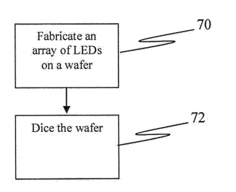
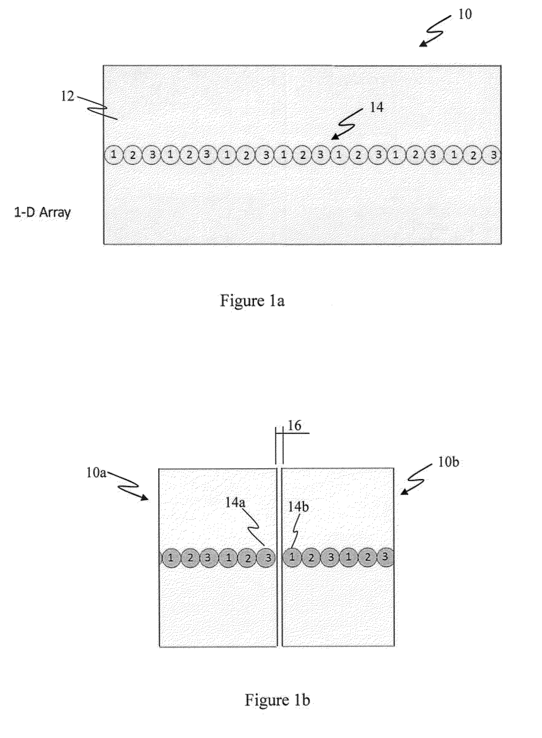
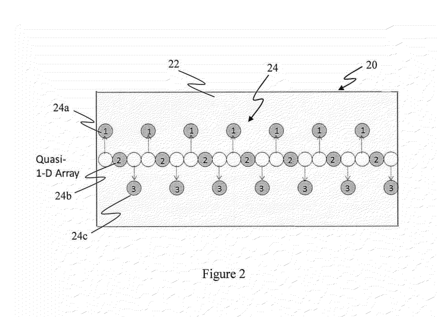
[0048]Generally disclosed herein are apparatus and methods to allow LED chips to be positioned adjacent one another to form a continuous array of LEDs while maintaining a constant pitch between individual LEDs.

[0049]LED arrays on an LED chip may comprise one or more of: 1) Discrete LED components (e.g. TO can, surface mount or epoxy packages) densely packed in a row on a PCB; 2) Bare die LED chips densely packed in a row (i.e. using Chip on Board (COB) or other approaches); and 3) Multiple individually addressable LEDs on a single chip (i.e. a monolithic LED array).

[0050]For the first two examples above, a full LED chip produces light and each LED device in an array may be considered a single emitter. Therefore, the size of the LEDs and the pitch of such LEDs in an array (and hence the resolution) is defined by the size and packaging density of the individual components. For example, if a standard bare die LED chip with dimensions of 250 μm×250 μm is used and requires a spacing of 2...


PUM


Abstract

An LED chip for use in an LED chip array forming a continuous array of LEDs. The LED chip comprises an array of LEDs on a substrate. LEDs in a row of the array are longitudinally offset from corresponding LEDs in another row. Adjacent LEDs in each row of the array are separated by a longitudinal pitch. At least part of an end face of the substrate is angled with respect to a transverse axis of the LED chip such that the LED chip is positionable adjacent another LED chip to maintain the longitudinal pitch between adjacent LEDs on different chips.

Description

CROSS-REFERENCE TO RELATED APPLICATIONS[0001]This application is a National Phase Application filed under 35 USC 371 of International Application No. PCT / EP2013 / 052690, filed on Feb. 11, 2013, which claims the benefit and priority from U.S. Provisional Patent Application No. 61 / 597,236, the disclosures of which are incorporated herein by reference in their entirety.TECHNICAL FIELD[0002]The present disclosure relates to a light emitting diode (LED) chip and a method of manufacturing an LED chip. More specifically, the present disclosure relates to, but is not limited to, LED chips and methods of manufacturing LED chips that may be placed adjacent one another to form continuous arrays of LEDs.BACKGROUND OF THE INVENTION[0003]LEDs are a form of semiconductor material that convert electrical energy into optical energy. In semiconductor LEDs, light is typically generated through recombination of electrons, originating from an n-type doped semiconductor layer, and holes originating from a...

Claims


Application Information

Patent Timeline
Patent Type & Authority Applications(United States)
IPC IPC(8): H01L27/15H01L33/62
CPCH01L33/62H01L27/153B41J2/45H01L25/0753H01L33/20B41J2202/50H01L2924/0002H01L27/156H01L2924/00H01L2924/12041H10K59/84H10K59/86H10K59/121H10K59/1216H01L25/50H01L2933/0033
Inventor HENRY, BILL
Owner META PLATFORMS TECH LLC
Why Eureka
Try Eureka