Liquid crystal display device and method for producing the same
a display device and liquid crystal technology, applied in liquid crystal compositions, instruments, chemistry apparatus and processes, etc., can solve the problems of display failure, overall response speed is insufficient, transmittance degradation caused, etc., to suppress ghosting, high response speed, and less drop marks
- Summary
- Abstract
- Description
- Claims
- Application Information
AI Technical Summary
Benefits of technology
Problems solved by technology
Method used
Image
Examples
example 1
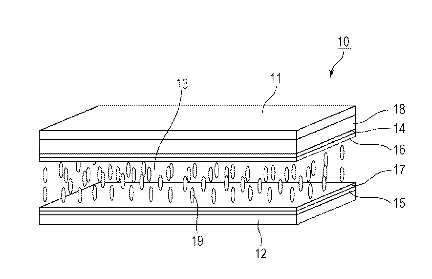
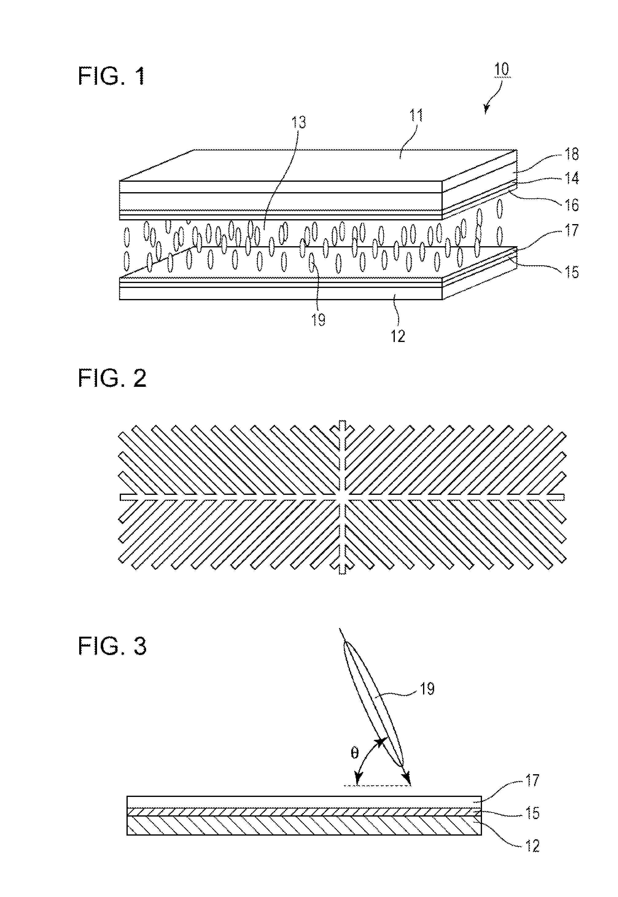
[0160]A first substrate (common electrode substrate) that has a transparent electrode layer constituted by a transparent common electrode and a color filter layer and a second substrate (pixel electrode substrate) having a pixel electrode layer that includes transparent pixel electrodes driven by active elements were made.
[0161]A vertical alignment film material containing a polymerizable liquid crystal compound and a polymerization initiator was applied to each of the common electrode substrate and the pixel electrode substrate by a spin coating method to form a 200 nm-thick precursor layer of a vertical alignment film. UCL-011-K1 (DIC Corporation) was used as the vertical alignment film forming material.
[0162]Each substrate with a vertical alignment film forming material applied thereon was heated in a 70° C. thermostat for 15 minutes to transform the polymerizable liquid crystal compound in the applied vertical alignment film forming material into an isotropic liquid.
[0163]The te...
example 2
[0189]A liquid crystal display device of Example 2 was obtained as in Example 1 except that a polyimide solution (trade name: JALS2131-R6, produced by JSR) containing 3% of a polyimide precursor and a solution containing 3% of a polymerizable compound having a reactive group represented by formula (V-2) below were used as the vertical alignment film forming material.
[0190]The liquid crystal display device of Example 2 was evaluated in terms of ghosting and drop marks as in Example 1. The results are shown in Table 8.
[0191]The results show that the liquid crystal display device of Example 2 was slightly inferior to the liquid crystal display device of Example 1 but exhibited high response speed, suppressed drop marks, and was resistant to ghosting.
TABLE 8Drop mark evaluationAAGhosting evaluationAResponse speed / ms8.7
example 3
[0192]A liquid crystal display device of Example 3 was obtained as in Example 1 except that a polyimide solution (trade name: JALS2131-R6, produced by JSR) containing 3% of a polyimide precursor and a solution containing 3% of a polymerizable compound having a reactive group represented by formula (V-3) below were used as the vertical alignment film forming material.
[0193]The liquid crystal display device of Example 3 was evaluated in terms of ghosting and drop marks as in Example 1. The results are shown in Table 9.
[0194]The results show that the liquid crystal display device of Example 3 was slightly inferior to the liquid crystal display device of Example 1 but exhibited high response speed, suppressed drop marks, and was resistant to ghosting.
TABLE 9Drop mark evaluationAGhosting evaluationAAResponse speed / ms8.8
PUM
| Property | Measurement | Unit |
|---|---|---|
| mass % | aaaaa | aaaaa |
| mass % | aaaaa | aaaaa |
| angle | aaaaa | aaaaa |
Abstract
Description
Claims
Application Information


