Light emitting diode assembly
- Summary
- Abstract
- Description
- Claims
- Application Information
AI Technical Summary
Benefits of technology
Problems solved by technology
Method used
Image
Examples
Embodiment Construction
[0043]Embodiments of the present invention will be described in more detail with reference to the accompanying drawings. It should be understood that the following embodiments are given by way of illustration only to provide thorough understanding of the invention to those skilled in the art. Therefore, the present invention is not limited to the following embodiments and may be embodied in different ways. Further, like components will be denoted by like reference numerals throughout the specification, and the widths, lengths, and thicknesses of certain elements, layers or features may be exaggerated for clarity.
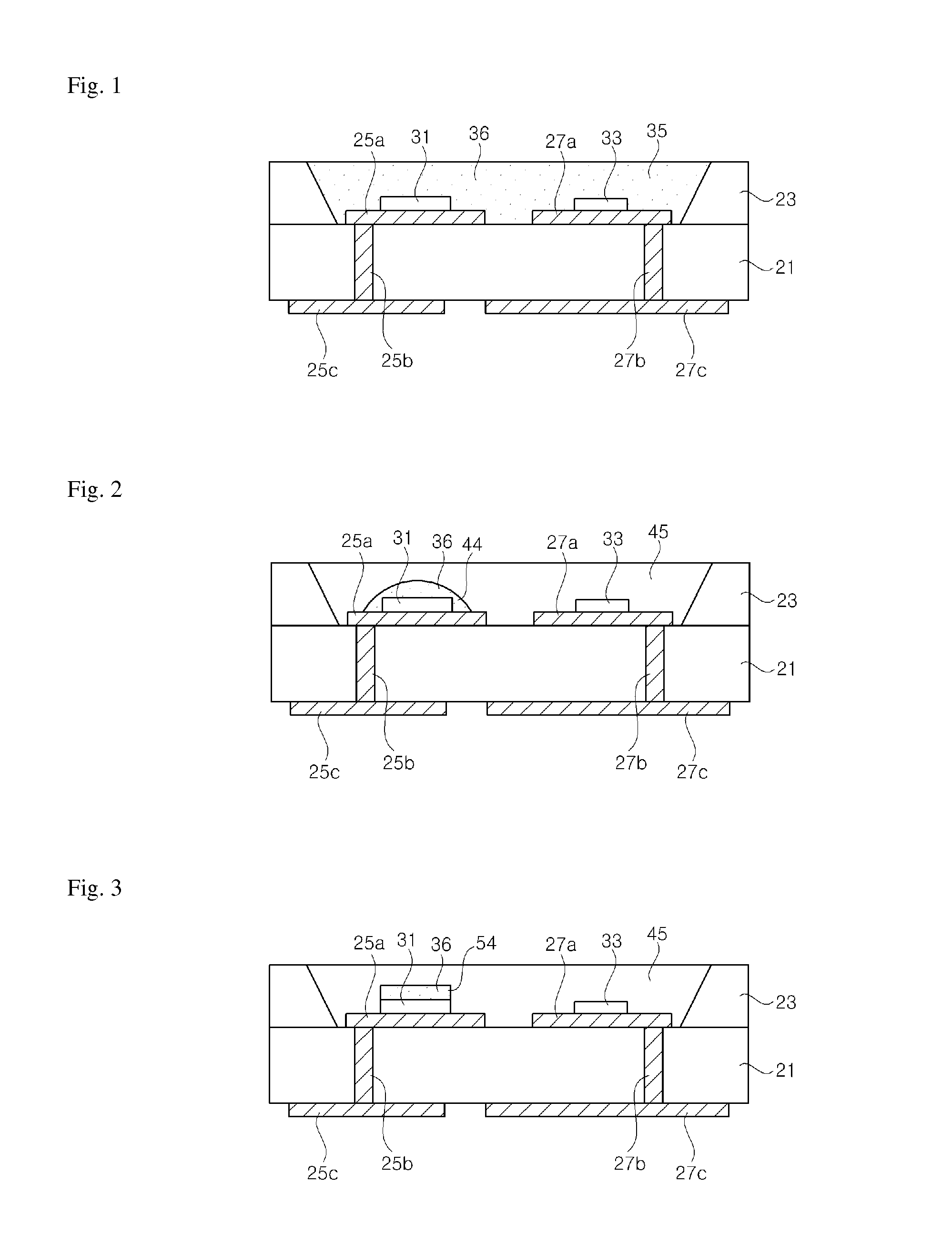
[0044]FIG. 1 is a schematic sectional view of a light emitting diode assembly according to one embodiment of the present invention.
[0045]Referring to FIG. 1, the light emitting diode assembly according to this embodiment includes a base substrate 21, a housing 23, a first landing pad 25a, a second landing pad 27a, a first via 25b, a second via 27b, a first external pad 25c, ...
PUM
 Abstract
Description
Claims
Application Information


